1. Introduction
Recently, as device processing enters the nanometer scale, device development based on nano-materials has received increasing attention [1-4]. Among various technical approaches, the "bottom-up" method emphasizes the rational construction of nano-functional devices based on atoms and molecules, which is regarded as the core of nanotechnology. Nanowire-based devices have shown great application potential in Field Effect Transistors (FETs), light-emitting diodes, sensors, nano-lasers and nano-generators, among others [3, 5-10]. In particular, III-V semiconductor nanowires are attracting great attention due to their excellent electrical and optical properties [11-12]. Among the many potential nanowire materials, In2O3 nanowires possess a wide bandgap of 2.8 eV and high field-effect mobility [13]. In2O3 nanowires are easy to prepare and can be produced in various ways including physical vapor deposition [14], hydrothermal methods [15], chemical vapor deposition [16], pulsed laser deposition [17] and molecular beam epitaxy [1]. Many previous studies mainly focused on the preparation and electrical properties of nanowires due to their beneficial properties such as chemical stability, excellent crystallinity, easily doping, low-cost synthesis, quantum confinement effect, and high quantum efficiency [1]. However, few studies have focused on their optoelectronic properties since the first report on the ultraviolet (UV) photodetection capabilities of In2O3 nanowires [18]. Despite recent advances, the performance of photodetectors still cannot meet practical demand.
This work presents a strategy to fabricate and suspend In2O3 nanowire devices. Through its unique design and relatively simple manufacturing process, an In2O3 nanowire channel can be separated from its substrate. The source and drain patterns are also defined by only one Electron Beam Lithography (EBL) step. Utilizing this device’s structure, we conducted an intrinsic study on the electrical characteristics of In2O3 nanowire FETs, exhibiting an on/off current ratio larger than 103, a Subthreshold Swing (SS) of 241.5 mV/dec and a low dark current of ~10−13 A. The calculated carrier mobility is approximately 54.6 cm2V−1s−1. The In2O3 nanowire photodetector exhibits a high photoconductive gain of 4.3 × 10³, a responsivity of 1.6 × 10⁵ A•W−1, and a specific detectivity of D* up to 9.3 × 10¹⁰ Jones at a low power density of 0.06 mW·cm−2(λ = 450 nm). The response time (rise time τr), which is defined as the time for the photocurrent to increase from 10% to 90% Ipeak, is about 150 ms. It is faster than In2O3 nanowire-based photodetectors that have been reported previously [19-20].
2. Device fabrication and characterization
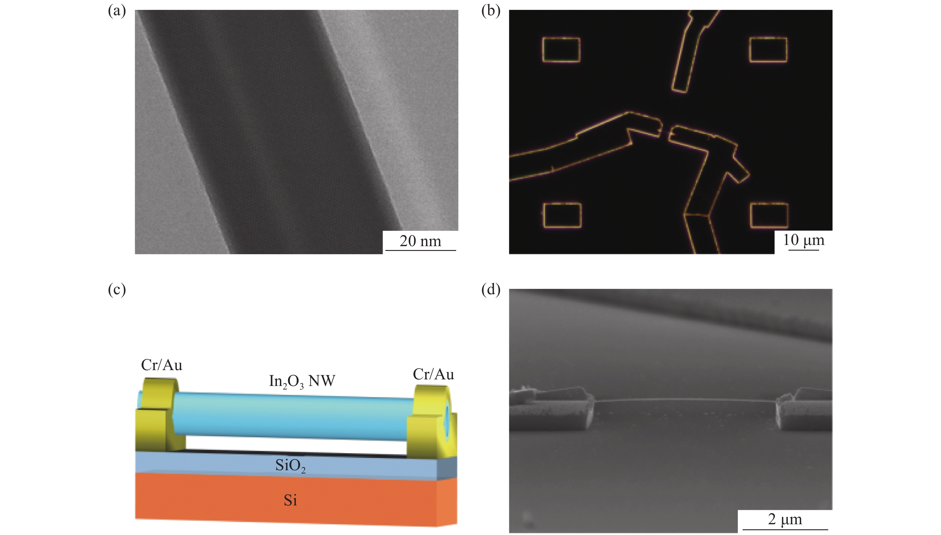
The In2O3 nanowires used in this study were synthesized by Chemical Vapor Deposition (CVD) through a Vapor-Liquid-Solid (VLS) growth mechanism. A mixture of high-purity In2O3 powder and graphite powder with a weight ratio of 5:1 was put into a quartz boat. A silicon substrate with a pre-deposition of 1-nm and an Au catalyst was placed downstream in the quartz tube to collect the products. A furnace was set to 1100 °C in 22 min and maintained for 1 hour under a constant flow of gas (argon/oxygen = 100:1, flow rate = 200 sccm). Finally, the system was left to naturally cool to room temperature. The TEM image in Fig. 1(a) shows that a large quantity of wire-like In2O3 microcrystals with good uniformity was fabricated by the CVD method. The diameter of the nanowire is approximately 50 nm. Fig. 1(b) and (c) show a dark-field microscopy image of the In2O3 nanowire FET and three-dimensional schematic view of the suspended single In2O3 nanowire photodetector. In2O3 nanowires used in this research were characterized by field-emission scanning electron microscopy and high-resolution transmission electron microscopy (HR-TEM, HT7700). The SEM result is shown in Fig. 1(d), confirming that the In2O3 nanowire is free of the substrate.
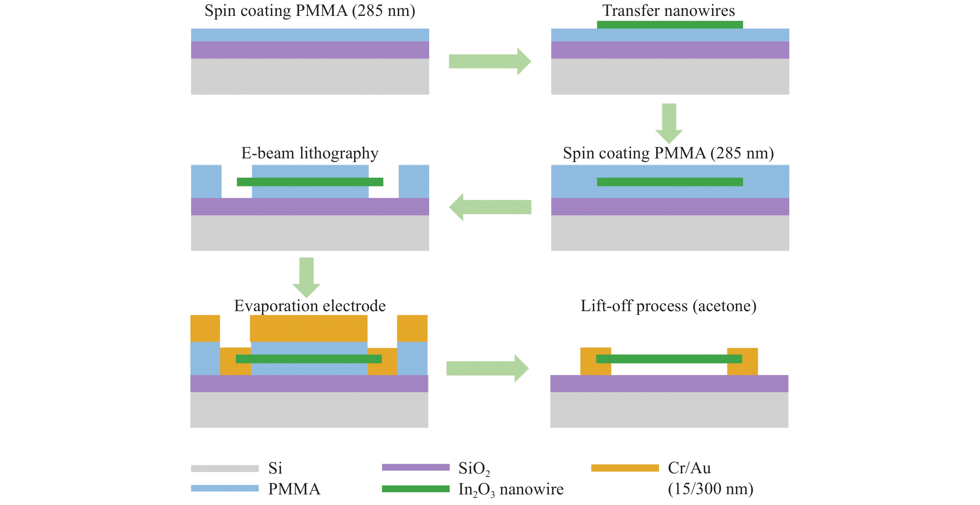
To fabricate suspended nanowire devices, the key part is to find a feasible way to fabricate a structure that is both suspended and stable. We found inspiration from previous work, which wrote about electron beam lithography on both poly-methyl-methacrylate (PMMA) and hydrogen silsesquioxane (HSQ) [21]. The process flow for preparing the suspended In2O3 nanowire FET is shown in Fig.2 (Color online). Specific steps are as follows: firstly, a layer of 280-nm-thick PMMA is spin-coated onto the Si/SiO2 substrate. Secondly, In2O3 nanowires are drop-casted onto the temporary layer of the spin-coated photoresist. The N-doped In2O3 nanowires produced by CVD have a typical length of 10 μm and a diameter of less than 100 nm. Thirdly another photoresist layer is spin-coated. Standard e-beam lithography is performed to define the electrodes on a marked In2O3 nanowire. Then, 15 nm chromium (Cr) and 300 nm gold (Au) are deposited using thermal evaporation. Finally, the fabrication of the device is finished after the lift-off process. To improve ohmic contacts, devices were annealed at 200 °C in Ar atmosphere for 2 hours.
3. Results and discussion
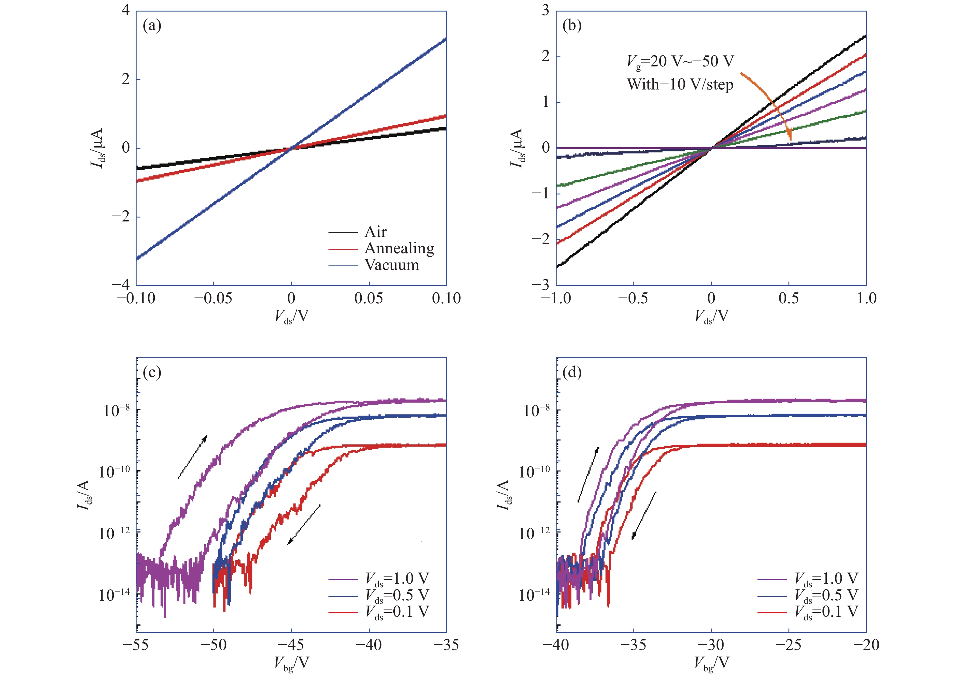
The electrical properties of fabricated suspended In2O3 transistors are investigated with a Lake Shore Probe Station together with an Agilent B1500 (Agilent Technologies, Santa Clara, CA, USA) semiconductor parameter analyzer. The I–V curves of the nanowire-based photodetector are shown in Fig. 3(a) (Color online) and indicate that different atmospheres can affect electrical conductivity. The annealing process can effectively improve the contact of metal electrodes. Under dark conditions, oxygen molecules tend to chemisorb onto the surface of In2O3 nanowire by trapping free electrons from the conduction band and then becoming negative ions O2–, which reduces the system’s free electron density. The larger current in a vacuum is a result of the lack of oxygen in such a test environment. Fig. 3(b) (Color online) shows the typical output characteristics of the device. The liner behavior suggests good ohmic contact between the nanowires and electrodes. As shown in Figs. 3(c) and 3(d) (Color online), low dark current (approximately 10−13 A) in both transfer curves can be attributed to the design of the suspended structure, which can effectively avoid the limitation of gate leakage current. Transfer curves of the same device in different atmospheres show a similar clockwise hysteresis performance. It can be confirmed that the curve does not significantly shift with an increase in drain bias for a static Vgs sweep range, which suggests ideal transistor characteristics for these suspended devices in a vacuum [22]. Compared with the sharp shift of transfer curves and higher turn-off voltage in air, this suspended design suggests applications in vacuum transistors are possible. The electron mobility μFE of a single In2O3 nanowire device can be calculated by using the expression μFE = gmL2/(CgVds), where the channel length L = 2.0 μm, and gm = dIds/dVgs is the transconductance of the nanowire device. Cg is the back-gate capacitance including the two parts that can be deduced based on the cylinder on-plane model: Cg1 = 2πε1εrL/[ln(4h1/d)] [22], where ε1εr is the dielectric constant of the air, h1(200 nm) is the height of suspension, and d(50 nm) is the In2O3 nanowire’s diameter. Cg2 =2πε2εrL/[ln(4h/d)], where ε2 is the permittivity of the SiO2, and h2 (280 nm) is the thickness of the SiO2 substrate. Vgs is the voltage between drain and source. The calculated carrier mobilities of the device in air and a vacuum are 12.4 cm2 V−1 s−1and 54.6 cm2 V−1 s−1, respectively. The system may be influenced by contact between nanowires and metal electrodes. The SS can be expressed by the equation SS = ∂Vg/∂(lgId), where Vg is the applied gate voltage and Id is the drain current. The SS value calculated in the different atmospheres is 324.7 mV/dec and 241.5 mV/dec, respectively. Previous work found that performance degradation is mainly attributed to the charge accumulation in the In2O3/SiO2 interface, and the gate coupling in the non-suspended structure is not as desirable as that in suspended couplings [13]. It is necessary to design gate dielectric and electrode systems to make a breakthrough in SS value limitation (60 mV/dec). The device shows a high on/off ratio that is larger than 103, which implies that this suspended device has immense potential in high-performance FETs.
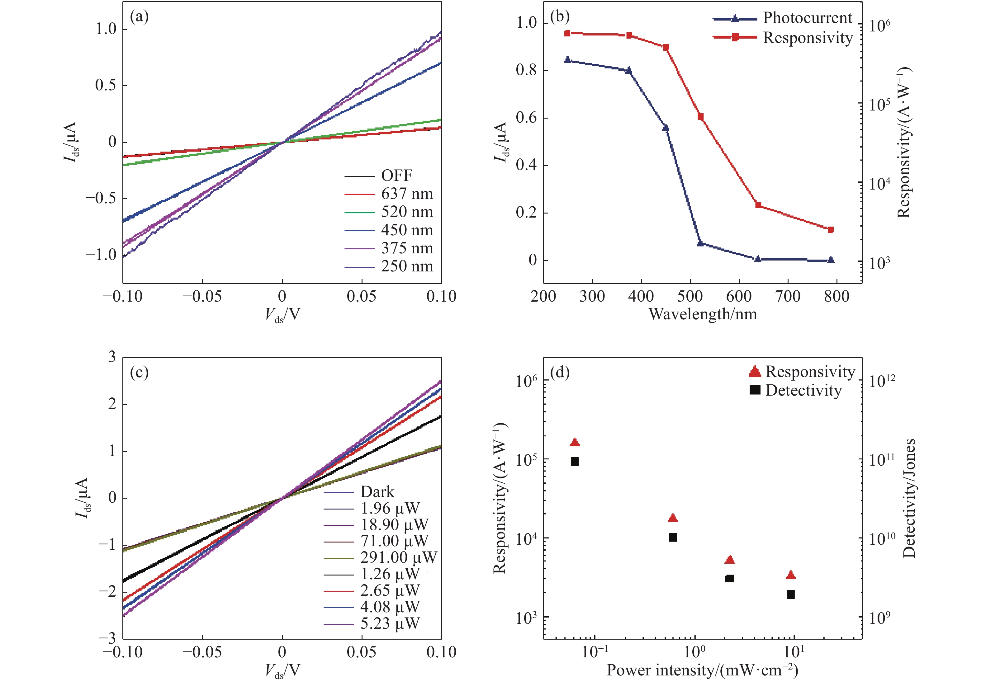
The spectral responsivity is measured using a series of laser sources (250, 375, 450, 520, 637 nm; Thorlabs, Inc) combined with Agilent B2902. The Ids-Vds characteristics of the photodetector were measured in the dark and different wavelengths of light, as shown in Fig. 4(a) (Color online). The dark current of the device is 0.12 μA. The light wavelengths of 637 nm and 520 nm (~1.10 mW·cm−2) have little influence on the device’s photocurrent compared to the dark current. Contrarily, as shown in Fig. 4(b) (Color online), the photocurrent increases drastically when the wavelength of incident light reaches to 450 nm, which has comparable energy to the bandgap of In2O3 (2.8 eV). The responsivity (R) can be defined as Iph/(PA), where Iph is the photocurrent, P is the incident power density, and A is the effective irradiated area on the nanowire. Fig. 4(b) also shows the dramatic responsivity difference (about three orders of magnitude) on either side of the wavelength corresponding to In2O3 bandgap. The value of R is as large as 1.6 × 10⁵ A·W−1 when incident light reaches the UV band with an applied voltage of 0.1 V. The results demonstrate the excellent photoresponsivity and wavelength selectivity of the In2O3 nanowire-based photodetector. The photoconductive gain (G), responsivity (R), and specific detectivity (D*) are the key parameters for evaluating the sensitivity of the photodetectors [23].
The corresponding external quantum efficiency (EQE) is defined as the ratio between the number of collected electrons and the number of incident photons [19]. It can be expressed by the following equation, EQE =Rhc/(eλ). The EQE of the device is calculated to be as high as (9.9 × 10⁷)% with irradiation of UV light (~ 200 nm). The high EQE is related to the exposure of the nanowire surface via the chemisorption/photodesorption of oxygen. It has been mentioned above that by trapping free electrons from the conduction band to becoming negative O2– ions, oxygen molecules tend to chemisorb onto the surface of an In2O3 nanowire in dark conditions, thereby reducing the free electron density O2(g) + e–→ O2–(ad) [19]. Electron–hole pairs are created in the bulk when illuminated with short-wavelength light. Due to the existence of new valence subbands, the photogenerated holes move from the bulk to the surface and these accumulated holes will react with the adsorbed oxygen ions, then release a captured free electron, h+ + O2− (ad) → O2 (g) [19]. Furthermore, separation of the structure between In2O3 nanowire and substrate caused ultrahigh surface-to-volume ratios and a free-standing interface, which played an important role in high R and EQE. Figure 4(c) (Color online) shows the Ids-Vds characteristics for different power intensities at a wavelength of 450 nm. The Ids-Vds curve shows a linear regime with increasing Vds. It could be predicted that there will be photon-generated carrier saturation and electron-hole recombination under strong light illumination if the bias and light intensity is large enough [24-26].
The specific detectivity is an important figure-of-merit characterizing the capability of the smallest detectable signal for a photodetector. Considering that the shot noise from the dark current is the major factor limiting the detectivity, the specific detectivity can be given by D* = RA′1/2/(2eIdark)1/2, where R is the responsivity, A′ is the effective area of the detector (A′ = L × d, L is the channel length, d is the nanowire’s diameter), e is the unit charge, and Idarkis the dark current. Figure 4(d) (Color online) shows the calculated values of responsivity and detectivity at different power intensities. The incident light’s power is calibrated with a PM100D power meter. It shows that R and D* increase dramatically with a decreasing light intensity, which can be caused by the trap states of the In2O3 nanowires. The R and D* of the photodetector are up to 1.6 × 10⁵ A·W−1 and 9.2 × 10¹⁰ Jones, respectively, under a low light intensity of 0.06 mW·cm−2. The highest responsivity is two orders of magnitude larger than that of commercial photodetectors based on Si, GaAs, and InGaAs [27]. Considering the small depletion of the intrinsic carriers in the nanowire channel, D* could be enhanced to up to 1015 Jones if further gate dielectric and electrode structures are built (to drive dark current down from 10−6 μA to 10−10 μA). The photo-conductive gain (G) is defined as the ratio between the number of charges collected by the electrodes per unit of time and the number of photons absorbed by the nanowire per unit of time (G = Ne/Nph). It can be calculated as G = (Iph/e)/(PA/hν), where Iph is the photocurrent, e is the electronic charge, P is the incident power density, A is the effective irradiated area, and hν is the energy of an incident photon. The G of the photodetector is up to 4.34 × 10⁵ under a low light intensity of 0.062 mW/cm−2, which is due to the long photon-generated carrier lifetime in the nanowire compared to the short carrier transit time between the electrodes [24, 26, 28]. High gain shows that large photocurrent output signals can be achieved with relatively low optical input.
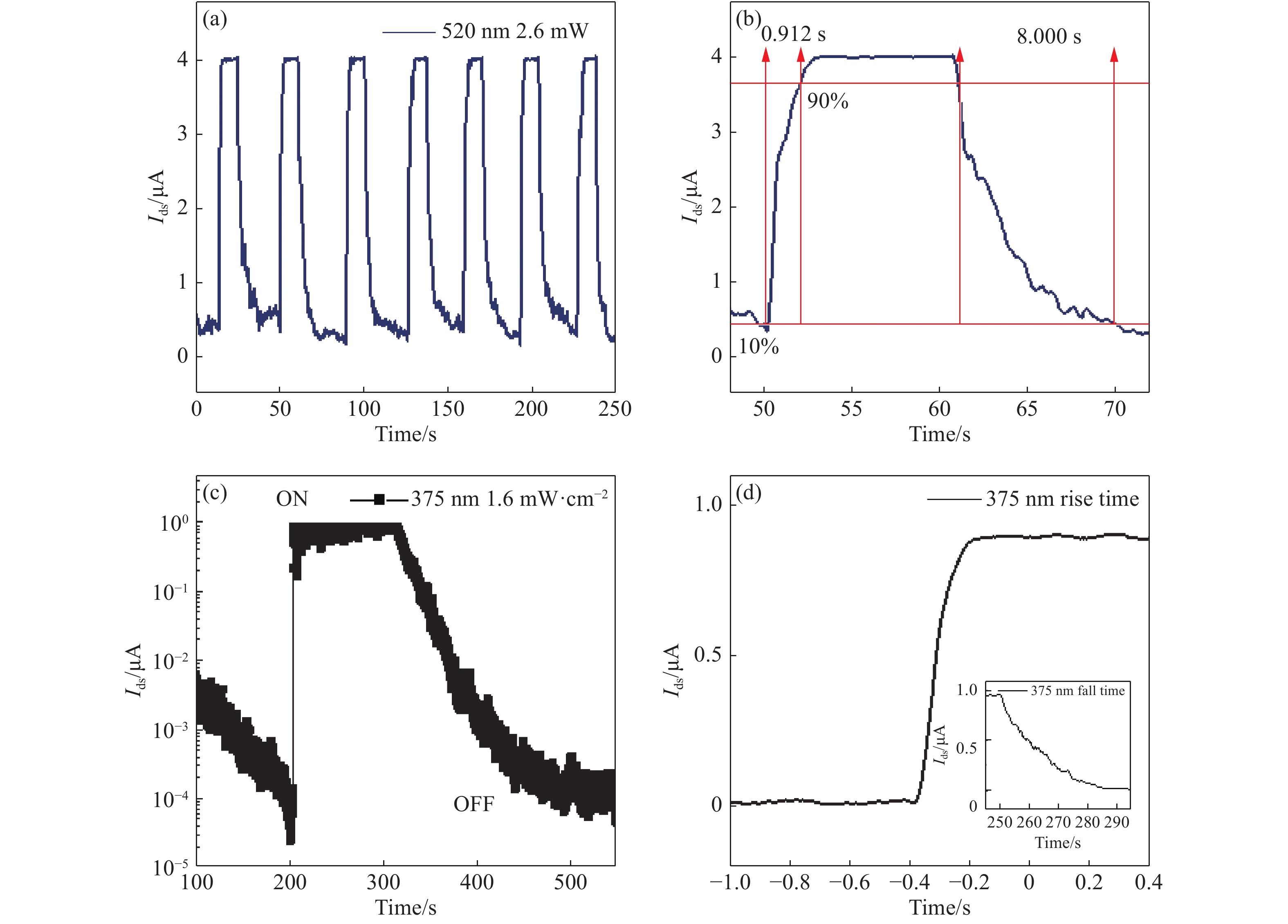
The repeatability and response speed are also important parameters for photodetection [29]. Time-resolved photoresponse measurements were performed to characterize the response speed of the photodetector when switching a green light on and off repeatedly (520 nm). The photocurrent responses under 520 nm of illumination with a back gate voltage of −30 V are shown in Fig. 5(a). The response time (rise time τr) and the recovery time (fall time τf), defined as the time for the photocurrent increasing (decreasing) from 10% to 90% (90% to 10%) of Ipeak (photocurrent peak), is 0.912 s and 8 s, respectively. This data is extracted with a Tektronix MDO3014. It shows high stability and reliability with the on/off photoswitching behavior at Vds = 1 V. As for the response speed characterization of UV light (375 nm) [25], a high-speed oscilloscope was used to monitor the fast-varying optical signal. Its longer recovery time may be related to the influence of the surface states [30]. The recombination of electrons and holes may be affected by the surface trap state of the nanowire after high-energy ultraviolet radiation. The rise time τr drops sharply to 150 ms, which is faster than previous reports for In2O3 nanowires photodetectors, to our best knowledge [19-20, 31]. This can be attributed to the reduction of the interaction effect between the nanowire and the substrate.
4. Conclusion
In summary, we have fabricated a suspended In2O3 nanowire transistor based on one-step EBL micro-nano processing technology that can stable and complete separation between a nanowire and a substrate. The intrinsic electrical transportation and photoresponse properties of In2O3 nanowire FETs are studied. The In2O3 nanowire transistors achieve a stable electrical property in a vacuum. Furthermore, this type of photodetector exhibits excellent optoelectronic performance including broad spectral responsivity, good repeatability, and fast response. Suspended nanowire structures provide an ideal way to investigate the intrinsic properties of nano-materials and broadens their applications in flexible and thermal isolation devices.

 DownLoad: