Key Laboratory for Micro-Nano Physics and Technology of Hunan Province, College of Materials Science and Engineering, School of Physics and Electronics, Hunan University, Changsha 410082, China
Mix-dimensional van der Waals heterostructures (vdWHs) have inspired worldwide interests and efforts in the field of advanced electronics and optoelectronics. The fundamental understanding of interfacial charge transfer is of vital importance for guiding the design of functional optoelectronic applications. In this work, type-II 0D-2D CdSe/ZnS quantum dots/MoS2 vdWHs are designed to study the light-triggered interfacial charge behaviors and enhanced optoelectronic performances. From spectral measurements in both steady and transient states, the phenomena of suppressed photoluminescence (PL) emissions, shifted Raman signals and changed PL lifetimes provide strong evidences of efficient charge transfer at the 0D-2D interface. A series of spectral evolutions of heterostructures with various QDs overlapping concentrations at different laser powers are analyzed in details, which clarifies the dynamic competition between exciton and trion during an efficient doping of 3.9×1013 cm−2. The enhanced photoresponses (1.57×10⁴ A·W–1) and detectivities (2.86×10¹¹ Jones) in 0D/2D phototransistors further demonstrate that the light-induced charge transfer is still a feasible way to optimize the performance of optoelectronic devices. These results are expected to inspire the basic understanding of interfacial physics at 0D/2D interfaces, and shed the light on promoting the development of mixed-dimensional optoelectronic devices in the near future.
Low-dimensional heterostructures are extremely important members in various semiconductor devices, including photodetectors, phototransistors and light-emitting devices1, 2. Recently, van der Waals heterostructures (vdWHs) based on 2D transition metal dichalcogenides (TMDs) have attracted world-wide attentions in the application of next-generation optoelectronic integrations beyond traditional silicon-based integrated circuits3, 4. Such 2D/2D vdWHs show unique properties, including high carrier mobility, atomic-scale depletion region and tunable light-matter interaction, which are stemming from the designed energy band alignment and the ultrafast interfacial charge transfer5-7. However, the interlayer coulomb interaction and the carrier scattering are dominant in such atomically-thin layers, which have great influences on the performance of optical behaviors and optoelectronic devices8. Besides, these kinds of devices still suffer from performance limitations due to their weak light absorption and pristine atom defects9.
Several strategies have been devoted to tackle these problems, such as surface chemical modification10, 11, nanophotonic structures integration12, 13, mixed-dimensional vdWHs design14, etc. The reduced dimension of semiconductors provides large specific surface areas and abundant interfaces, which means, TMDs flakes integrated with one-dimensional (1D) nanowires, especially with 0D quantum dots (QDs), could perform as promising architectures for high-performance optoelectronic devices15-18. To further achieve the high optoelectronic performance of mixed-dimensional vdWHs device, the integration of 2D materials with high carrier mobility and 1D or 0D materials with large light-sensitive absorption should be designed and fabricated. The reduced dimension creates abundant interfaces providing alternative channels to generate highly-efficient charge doping at the interface of 0D/2D semiconductors19, 20. 0D QDs possess high quantum efficiencies, strong absorption coefficients, and low-cost processings, which are usually utilized to construct mixed-dimensional devices exhibiting broadband photodetection, excellent stability and remarkable photoresponsivity21.
Molybdenum disulfides (MoS2) monolayers are typical TMD semiconductors with band energy of 1.83 eV in visible spectral range, which usually show room temperature mobility of 0.1–10 cm2·V−1·s−1, photoresponsivity of <10 A·W–1 and on-off ratios of 106–108 22, 23. Perovskite QDs, such as CH3NH3PbBr3 and CsPbBr3, have recently been studied to build mixed-dimensional heterostructures with MoS2 flakes showing enhanced optoelectronic responses24-26. But they face challenges in realizing air-stable heterostructures27. Besides, the design of heterostructure type among type-I and type-II is crucial, which decides carrier transfer behaviors and photoresponse enhancements25, 28. Colloidal QDs and their core-shell QDs are stable semiconductors, which have been applied on MoS2 layers to realize high-performance photodetectors29, 30. Although these 0D/2D conceptual devices show outstanding performances in phototransistors and photodetectors, the charge transfer at the mixed-dimensional interfaces with complex ultrafast processes remains poorly understood31-33. Moreover, the light-controlled charge transfer processes in 0D/2D vdWHs have less been investigated, which may stimulate the design and creativity of photosensitive transistors.
In this work, we design 0D/2D mix-dimensional vdWHs (CdSe/ZnS QD/MoS2) to investigate the light-triggered charge transfer processes at the nanoscale interface. The steady-state and transient-state optical measurements of colloidal QDs, MoS2 monolayers and heterostructures are systematically investigated, showing tunable PL spectra and ultrafast charge transfer stemmed from a type-II band alignment. In a three-energy-level model, an effective charge transfer from QDs to MoS2 monolayers can be verified from the weight ratio of exciton spectra, which has been estimated as 3.9×1013 cm−2. The competition of QD exciton, MoS2 exciton and trion can be further modulated in a light-triggered n-type doping process. Moreover, these power-sensitive charge transfer processes at the interface help to improve the performance of optoelectronic devices based on TMDs with large responsivities and detectivities. These results are expected to provide the fundamental understanding of light-triggered charge transfer in 0D/2D mixed-dimensional vdWHs, which will contributes to the designing of high-performance optoelectronic devices in the near future.
Materials and methods
Material preparation
MoS2 monolayers were synthesized by chemical vapor deposition method. A quartz boat was filled with molybdenum oxide (MoO3) powder and then located in the center of a furnace. The boat was covered by a cleaned Si/SiO2 substrate. Another ceramic boat filled with sulfur (S) powder was placed at the upstream region of the furnace in a lower temperature zone. The temperature was raised to 830 °C for 10 min to grow MoS2 crystals. Meanwhile, the S powder was heated to 300 °C by a heating belt, and the sulfur vapor flowed into the furnace by the carrier gas of Ar. Finally, the furnace was gradually cooled down to room temperature. During the whole process, the ultrahigh-purity Ar gas was held at 75 sccm under atmospheric pressure. Colloidal CdSe/ZnS QDs are commercially available. The heterostructures were fabricated in a spin-coating process, where dilute solutions of 0.025 mg/L QDs can be spin-coated onto the MoS2 monolayer at a rotation speed of 2700 rpm for 1 min.
Optial characterization
The optical properties were measured by a home-built μ-PL system. An iHR550 Raman spectrometer from Horiba was utilized to measure the PL and Raman spectra with 300 g·mm−1 and 1200 g·mm−1 gratings, respectively. A Ti: Sapphire laser at 400 nm (100 fs, 80 MHz) was used as the excitation source for transient-state measurements, which was generated by an 800 nm laser from a mode-locked oscillator (Tsunami 3941-X1BB, Spectra- Physics) positioned after a BBO crystal. Time-resolved PL (TRPL) is measured by a streak camera (Hasmamatsu Universal, C10910) with a resolution of ~3 ps for short-time range measurements (~200 ps). A 532 nm solid-state laser was also induced to excite samples to obtain the steady-state spectra. The objective lens is 50× magnifications, and the diameter of the laser spot is ~2 μm.
Device fabrication and measurement
The metal electrodes of MoS2 and heterostructure devices were fabricated in a typical E-beam lithography (EBL) process, followed by e-beam evaporation of Au/Cr (100 nm/5 nm) electrodes. Then, samples were annealed in vacuum for 3 h at ≈180 °C to improve the contact conductance. The surface ligands of the coated QDs were purified by ethyl acetate and hexane to facilitate charge transport. Finally, the devices were annealed on a hot plate at 50 °C for 10 min to evaporate the solvent for electrical measurements. The electrical and optoelectronic properties of the as-fabricated devices were performed in a vacuum Lake Shore Probe Station combined with an Agilent B1500A semiconductor analyzer at room temperature.
Results and discussion
Figure 1(a) shows the schematic view of QD/MoS2 heterostructures under the excitation of a laser. MoS2 flakes were grown on SiO2/Si substrate in a chemical vapor deposition (CVD) process. To fabricate mixed-dimensional 0D/2D vdWHs, a drop of solution with 0.025 mg·L−1 CdSe/ZnS QDs was then dropped onto a prepared CVD-grown MoS2/SiO2/Si substrate. The density of QDs on substrates can be controlled by choosing the number of spin-coating times. From the optical images of pure MoS2 flakes and 0D/2D vdWHs (Supplementary information S1), it can be obviously observed that the optical contrast of MoS2 flakes varies when QDs are overlapped.
Figure 1.Schematic view and TEM characterizations of MoS2 monolayer and CdSe/ZnS QDs. (a) Schematic view of mixed-dimensional QD/MoS2 heterostructures on SiO2/Si substrate under the excitation of a laser. (b) High-resolution TEM (HRTEM) image of MoS2 monolayer with the scale bar of 5 nm. The inset shows the corresponding selected area electron diffraction (SAED) pattern, where the diffraction points are arranged in a hexagonal structure. (c) Enlarged FFT image of the marked area in a rectangular region in (b). The lattice spacing is 2.78 Å. (d) The AFM image of MoS2 monolayer with clear surface, and the height of MoS2 is observed to be 0.75 nm. Low-resolution (e) and high-resolution (f) TEM images of QD/MoS2 heterostructures, where scale bars are 100 nm and 20 nm, respectively. The red arrows and circles in (e) are QDs on MoS2 monolayer, and the orange arrows in (f) are the wrinkles of MoS2 flakes. (g) The HRTEM image of QD/MoS2 structures with a scale bar of 2 nm. Inset shows two sets of SAED patterns.
The structure and morphology of as-prepared QD/MoS2 heterostructures can be confirmed by transmission electron microscopy (TEM) and atomic force microscopy (AFM). Figure 1(b) shows the high-resolution TEM image of MoS2 monolayer. Our MoS2 samples are of high-quality that there are no defects or substitute atoms observed from measurements. The inset shows the corresponding selected area electron diffraction (SAED) pattern. The pattern only presents one set of six-fold symmetry diffraction spots, which is stemming from the hexagonal atom arrangement of MoS2 flakes. The enlarged high-resolution TEM (HRTEM) image is shown in Fig. 1(c), which is derived from the marked squares in Fig. 1(b). The interplanar spacing is measured to be 2.78 Å corresponding to (100) planes of hexagonal MoS2. AFM topography of MoS2 monolayer shows a clear triangular shape, and the thickness is determined to be 7.5 Å (1 Å=10−10 m).
After the wetting transfer process, QD/MoS2 heterostructures can be successfully transferred onto the Cu grid. Figure 1(e) shows the low-resolution TEM image of QD/MoS2 heterostructures, where QDs are randomly distributed on the surface of MoS2 monolayer, which have been marked by the red arrows. The scale bar is 100 nm. From a HRTEM image with the scale bar of 20 nm, the diameters of QDs are ranging from 8−15 nm (Fig. 1(f) and Supporting Information S2). Notably, the wrinkles or the edges of MoS2 monolayer are clearly observed as orange arrows point, which confirms that the as-transferred films are intact. From an enlarged area of HRTEM image of QD/MoS2 heterostructure (Fig. 1(g)), Moiré patterns can be observed at the edge of QDs, which is caused by overlapping lattices between MoS2 and QDs. The scale bar is 2 nm. The corresponding SAED image shows two different sets of arranged diffraction patterns, as shown in the inset of Fig. 1(g). The orange circles show a six-fold symmetry diffraction spots from MoS2, while the red circles exhibit a parallelogram configuration from CdSe/ZnS QDs.
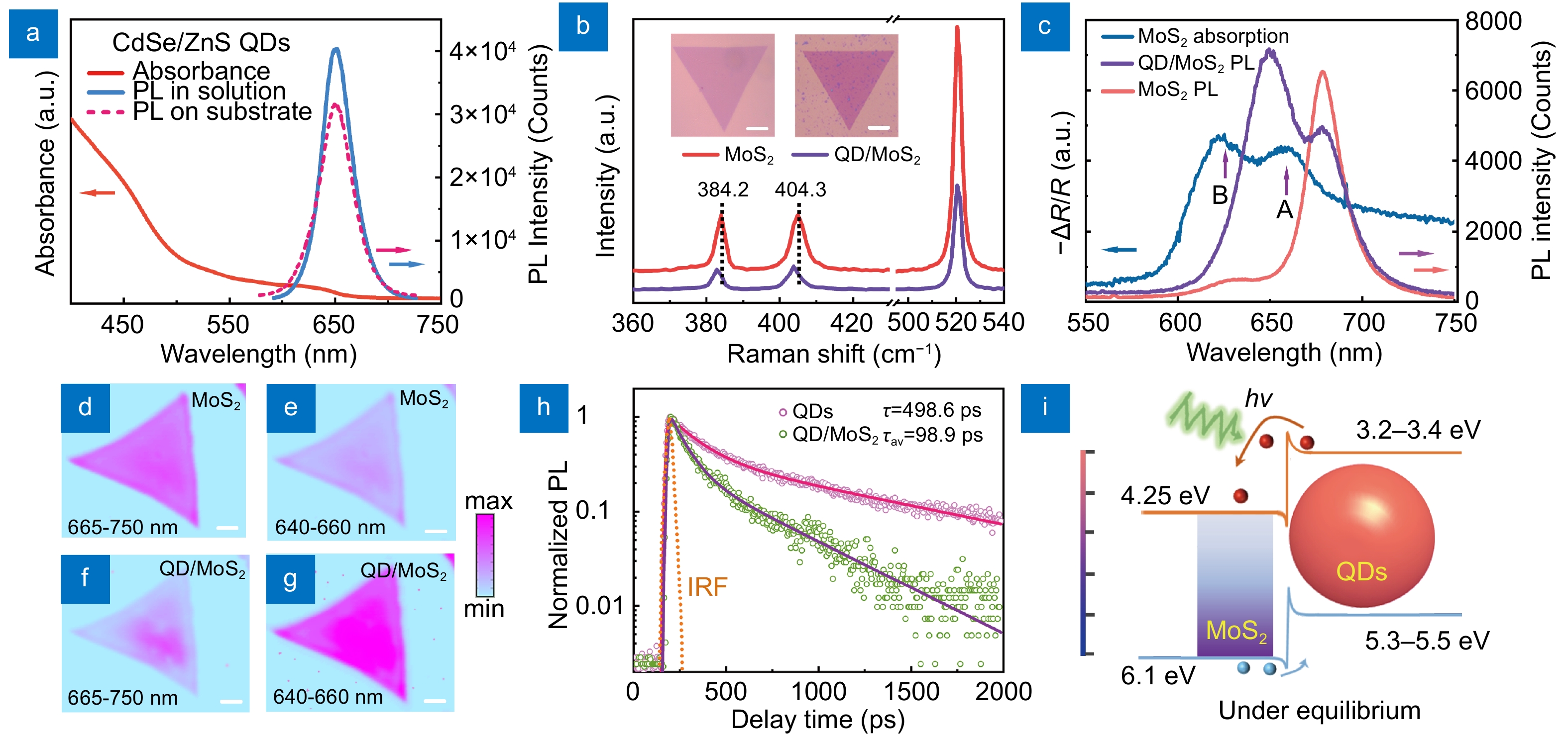
The optical and spectral properties have been investigated among CdSe/ZnS QDs, MoS2 monolayers and their heterostructures. Figure 2(a) shows the UV-visible absorption spectrum of QDs solution, where two dominant absorption peaks are observed at around 450 nm and 620 nm. The PL spectra of QDs solution (0.2 mg·L−1) and QDs film on SiO2/Si substrate show Lorentzian lineshapes, where the peak center is 650 nm with a full width at half maximum (FWHM) of 45 nm. Although the excitation conditions are different, the PL spectrum of QDs on substrate exhibits a slightly-stronger spectral broadening than QDs in solutions. It is because of the change of the dielectric environment of exciton emissions.
Figure 2.Optical and spectral characteristics of QDs, MoS2 monolayer and mixed-dimensional vdWHs. (a) The UV-visible absorption spectrum (orange) of CdSe/ZnS QDs in 0.2 mg·L−1 solution. PL spectra of QDs in solution (blue) and on SiO2/Si substrate (dotted line). (b) Raman spectra of MoS2 monolayer and QD/MoS2 heterostructures. E12g and A1g modes are 384.2 cm−1 and 404.3 cm−1 for MoS2 monolayer, respectively, and the E12g peak shifts blue to 383.3 cm−1 in heterostructures. Insets present the optical microscopy images of MoS2 monolayer and heterostructure. The scale bars are 6 μm. (c) The absorption (black) and PL (red) spectra of MoS2 monolayer. The PL intensity maps of MoS2 monolayer are measured at the spectral ranges of (d) 665−750 nm and (e) 640−660 nm. The PL intensity maps of heterostructures with 0.025 mg·L−1 QDs are measured at the spectral ranges of (f) 665−750 nm and (g) 640−660 nm. All the scale bars in mapping images are 5 μm. (h) Time-resolved photoluminescence (TRPL) spectra of QDs and QD/MoS2 heterostructures. The average lifetimes of QDs and heterostrutures are 498.6 ps and 98.9 ps, respectively. (i) The schematic view of energy band for QD/MoS2 heterostructures under the light excitation.
Figure 2(b) shows the Raman spectra of MoS2 monolayer (red curve) and QD/MoS2 heterostructures (purple curve). Two typical Raman peaks of MoS2 monolayer are observed at 384.2 cm−1 and 404.3 cm−1, which correspond to the E12g and A1g vibrational modes, respectively. The difference between these modes in the as-synthesized MoS2 monolayer is approximately 20.1 cm−1, which is slightly larger than the mechanically exfoliated monolayer MoS2 because of the crystalline strain34, 35. While in heterostructures, the Raman peaks of E12g and A1g modes blue-shift lightly, which are arising from the strain force and the charge transfer at the interface of heterostructures. The peak intensity of heterostructures shows a great attenuation, which is due to the blocked signals by the overlapped QDs layer. Insets show two optical images of MoS2 monolayer (left) and QD/MoS2 heterostructures (right), and scale bars are 6 μm.
The absorption spectrum of MoS2 monolayer is measured as shown in Fig. 2(c), which is derived from the differential reflectance spectra between MoS2/substrate and substrate under white light illuminations. Two absorption peaks are observed to be located at approximately 622 nm and 659 nm, which correspond to direct excitonic transitions at K points in the Brillouin zone of MoS2. Correspondingly, the PL spectrum of MoS2 monolayer presents two featured peaks at 630 nm and 678 nm, respectively. In 0D/2D vdWHs, PL spectra show two peaks at 650 nm and 677 nm14, 36. The peak intensity of exciton A decreases much, because charge transfer behaviors occurring at the interface suppress the radiative recombination. The PL spectra are excited by a 532 nm laser at 0.3 mW, and the detected samples are heterostructures with 0.025 mg·L−1 QDs.
PL intensity mapping has been performed to show spectral change in MoS2 monolayer and heterostructures. Figure 2(d) and 2(e) show the images of PL mapping of MoS2 monolayer at 665−750 nm and 640−660 nm, respectively, which are consistent with PL peaks of QDs and exciton A of MoS2. It is obviously observed that the PL intensity is dominant at the spectral range of exciton A. Images of PL intensity mapping of vdWHs are shown in Fig. 2(f) (665−750 nm) and Fig. 2(g) (640−660 nm). In comparison to Fig. 2(d), the PL intensity of heterostructure in Fig. 2(f) decreases a little owing to the interfacial charge transfer, and the intensity distribution shows slight inhomogeneity. While at the detection wavelength of 640−660 nm, the intensity of heterostructure is slightly stronger than that of MoS2 monolayer, where the intensity enhancement is mainly from the high-efficiency emission of QDs. Besides, a few QDs islands distributed on the substrate can also be observed. The laser powers are controlled at 0.3 mW for all the mapping measurements, and all the scale bars in Fig. 2(d−g) are 5 μm.
Time-resolved photoluminescence (TRPL) spectroscopy was carried out to further study and understand the spectral quenching caused by charge transfer. Fluorescence lifetime detection were obtained with 0.4 mg L−1 QD/MoS2 samples excited by a pulsed laser (400 nm, 80 MHz), at an excitation power of 0.3 mW. The signals were subsequently filtered by 650/50 nm bandpass filters, which can collect the full PL spectral range of QDs while keeping away from the main PL peak of MoS2 monolayer. The PL lifetimes for the two samples in Fig. 2(h) can be fitted and estimated using a biexponential decay model (). The decay processes are considered to be consisted of fast decay τ1 and slow decay τ2. The fast decay is related to the trap-assisted recombination in QDs or carrier extraction by the layers in heterostructures, while the slow decay is related to radiative recombination37, 38. By analyzing the components of two decay processes, the average lifetime of QDs and QD/MoS2 heterostructures are determined to be 498.6 ps and 98.9 ps, respectively. The average lifetime of QD/MoS2 heterostructure decreases much compared to QDs, indicating that considerable charge transfer can occur at the 0D/2D interface. Notably, the QDs in heterostructures exhibit a larger proportion of the fast decay than that exhibited by QDs alone, which confirms the trap-assisted recombination or carrier extraction is induced and dominant in QD/MoS2 heterostructures due to the charge transfer process (Supporting Information S3).
Figure 2(i) shows the energy band diagram of QD/MoS2 heterostructures. The conduction band and valence band of MoS2 monolayer are reported to be 4.25 eV and 6.1 eV in previous work, respectively26. While for QDs, the conductance and valence bands are reported to be 3.2−3.4 eV and 5.3−5.5 eV, respectively39, 40. The energy band structure of QD/MoS2 heterostructure is determined to be a type-Ⅱ band alignment. The built-in field is realized due to the interfacial charge transfer. With the excitation of incident laser, electron-hole pairs are mainly generated in the highly light-absorbing QDs layer, and then separated by the built-in field. As a result, electrons drift to the MoS2 layer while holes are left in QDs.
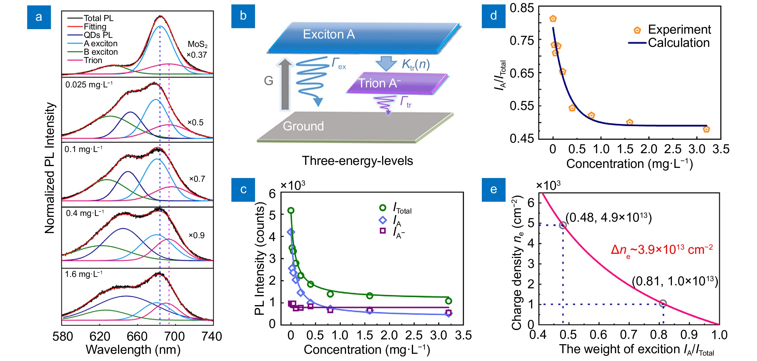
To estimate the charge doping efficiency in heterostructures at various concentrations, the analysis of spectral evolution are performed to demonstrate the contribution of both exciton and trion in the PL spectra. Figure 3(a) shows the competition between exciton and trion emissions when the QD concentration is increased. At low concentrations, the exciton components are dominated in the total spectra, while the weight of exciton decreases as the concentration increases. All the components are fitted using Lorenze line-shaped peaks (Supporting Information S4).
Figure 3.Analysis of PL spectral evolution of heterostructures at various doping densities. (a) Normalized PL spectra of QD/MoS2 heterostructures with different QD concentrations. The total PL spectra (red) can be fitted well with several components, involving QD exciton (dark blue), MoS2 exciton A (blue), trion (pink) and exciton B (green). (b) Schematic view of the three-energy-levels including exciton, trion and ground states, where the trion is generated from the exciton. (c) Diagram of PL intensity of total intensity (ITotal), exciton (IA) and trion (IA-). Fitting curves match well with experimental results. (d) The weight ratio of exciton (IA/ITotal) as a function of concentration. (e) Calculations of charge density (ne) based on the law of mass action model. The electron density of charge transfer (Δne) is determined as 3.9×1013 cm−2.
The three-energy-levels model is shown in Fig. 3(b) to illustrate the competition between exciton and trion. Exciton is excited from the ground state to exciton energy level under the laser excitation (G). In an assumption that the trion is generated from the exciton in a non-radiative channel (Ktr(n)). Both the exciton (Γex = 0.002 ps−1) and trion (Γtr = 0.02 ps−1) in MoS2 monolayer generate PL signals in radiative channels. Then, the rate equations for the population of exciton (NA) and trion (NA’) can be expressed as
(1)
(2)
(3)
where Ktr (n) is the formation rate of trion that relates with the QDs concentration (n), and Ktr (0) = 0.5 ps−1 is the formation rate of trion for the pure MoS2 film41. The minimum ktr (δ) can be obtained as 0.02 ps−1 as reported before. α is a parameter that reflects physical adsorption probability of QDs (Supporting Information S5)42.
Figure 3(c) plots the changing trend of total PL intensity, exciton and trion at various concentrations. Both the total PL intensity and the exciton intensity attenuate greatly as the concentration increases. Because the charge transfer electrons become abundant with high QDs concentrations, the recombination process of electron-hole pairs is deeply suppressed. However, the intensity of trion is almost unchanged in the doping process, which is due to the Pauli blocking effect and many-body interactions that the luminescence of the trion is easily saturated at low doping levels43, 44. The weight ratio of exciton in total PL (IA/ITotal) at different concentrations can be obtained from Fig. 3(c), where the ratio gradually decreases from 0.81 to 0.48 when the concentration increases, as shown in Fig. 3(d). Based on the mass action law, the charge density can be estimated from the weight ratio of exciton. Figure 3(e) shows the dependence of charge density with the weight ratio. The estimated charge density of MoS2 monolayer is ~1×1013 cm−2 due to the vacancy-induced electron doping45. With 3.2 mg·L−1 QDs doping, the charge density of heterostructure can be calculated as 4.9×1013 cm−2. Finally, the estimated density of doped electrons (Δne) is 3.9 × 1013 cm−2, which confirms that n-type doping happens at the interface of QDs and MoS2 (Supporting Information S6). Notably, this light-induced doping is at the same level of electric gating and chemical adsorption doping (~1013 cm−2)46, 47.
To further study the modulation ability of light-induced charge transfer and competitive exciton emissions, the laser-power dependent spectra of QDs, MoS2 and heterostructures with 0.025 mg L−1 QDs have been systematically investigated. Figure 4(a) and 4(b) show power-dependent PL spectra of MoS2 and QDs, respectively. When laser powers are increased from 65 to 670 μW, the intensity enhancement factors are determined as P=I/I0, where I and I0 are the intensities detected at high and low laser powers, respectively. P are detected as 8.4 for MoS2 exciton A and 7 for trion, respectively (Supporting Information S7). While for QDs, the intensity enhancement factor is detected as 20, and peak positions are stably appearing at 650 nm.
Figure 4.Laser-power dependent spectral modulation of QDs, MoS2 and their heterostructures. PL spectra change of (a) MoS2 monolayer and (b) QDs at various laser powers. (c) Analysis of PL spectral shapes in QD/MoS2 heterostructure with the excitation of various laser powers. The total PL peak consists of QD exciton (green), MoS2 exciton (A, blue), trion (A-, purple) and B exciton, and they can be fitted well in the shape of Lorentzian curves. (d) Plots of normalized PL intensity of exciton and trion as a function of laser powers. The relationship of PL intensity (I) and laser power (P) can be fitted as I=(P)m. (e) Schematic of exciton generation and emission at low and high laser powers.
Figure 4(c) shows the PL spectral evolution of QD/MoS2 heterostructures with increasing laser powers ranging from 65 to 670 μW. There is an obvious competition between QD exciton (green), MoS2 exciton A (blue) and trion (purple). At low power densities (<120 μW), MoS2 exciton and trion emissions are dominant resulting in a higher PL intensity larger than QDs. When laser powers are further increased, all components of exciton and trion get stronger, but the increasement speed behaves differently. It can be observed that the component of QDs exciton increases much fast, which gets stronger and becomes comparable to the component of MoS2 exciton at about 120 μW (Supporting Information S8).
The evolution of peak intensity of exciton and trion with laser powers has been plotted in Fig. 4(d). Both x-axis and y-axis are presented in log scales. The relationship of PL intensity (I) and laser power can be approximately written as I=(P)m, where m denotes exponent. For QD exciton, m decreases from 1.28 to 1.15 (QDs exciton in heterostructures). The value of m obtained from exciton A of MoS2 decreases from 0.9 to 0.87 (exciton A in heterostructures). The difference of PL sensitive-response gives rise to the competition and spectral evolution at various light powers. Figure 4(e) shows the schematics to illustrate the light-controlled spectral change. The blue rectangular and dotted orange rectangular show the areas of MoS2 flakes and QDs films, respectively. In a QD/MoS2 heterostructure with low QD density (as shown as the overlapping region), the number of MoS2 excitons excited at low laser powers is larger than QDs excitons. However, when the laser powers are increased to a high level, more QD excitons are generated, which are comparable to the contribution of MoS2 excitons, or even larger than that. The light-controlled spectral evolution shows the potential ability of tunable light-matter interactions in TMDs, which helps to influence the performance of optoelectronic devices.
The photo-induced charge behaviors are crucial to improve the performance of optoelectronic devices. The phototransistors of pristine MoS2 and vdWHs are systematically investigated, and their characteristics of photocurrents are measured to investigate the influence of interfacial charge doping. Figure 5(a) shows the schematic view of the device, where MoS2 monolayer served as a channel in the mix-dimensional FET (field-effect transistor), and Au/Cr (100 nm/5 nm) metal served as source/drain contacts on the back-gate Si/SiO2 substrate. Under the light illumination, electrons from QDs are transferred into MoS2 monolayer resulting in an efficient charge doping. The dilute solution of QDs can be uniformly spin-coated onto the MoS2 monolayer to realize the mixed-dimensional vdWHs device.
Figure 5.Optoelectronic performance of the vdWHs phototransistor compared with a pristine MoS2 phototransistor. (a) Schematic view of the phototransistor device, and the inset is an optical image of the as-prepared device with the scale bar of 10 μm. (b) Transfer characteristics of two devices in the dark and under the illuminations (from 0.11 nW to 34.75 nW) at Vds=1 V. (c) Transfer characteristics in dark (dotted line) and under the illumination (solid line, Peff = 34.7 nW) at Vg=0 V. (d) Photoresponsivities and (e) specific detectivities of two devices as a function of effective powers at Vg=60 V, respectively. (f) Time-dependent photoresponses under the pulsed illumination powers (from 0.11 nW to 19.78 nW) over multiple cycles at Vds=1 V. (g) The rise and fall times in photocurrent extracted from figure (f) under the illumination of 0.11 nW. (h) The photocurrent curves of vdWHs device with various QDs concentrations.
To evaluate the optoelectronic performance of the vdWHs device compared to that of the MoS2 transistor, we investigated the photo-induced transfer curves (Fig. 5(b)), as well as the current–voltage characteristics in the dark and under illuminations (Fig. 5(c)). Both pristine MoS2 and hybrid phototransistors exhibit a typical n-type behavior in the dark. The threshold voltages of pristine MoS2 and heterostructure phototransistors are obtained as −20 V and −60 V. As shown from the photoinduced transfer curves (Ids−Vg) under the illumination (520 nm), Ids of the photodetector in the dark is increased by ~4.8 times compared to that of the pristine MoS2 device (7.55×10⁻⁷ A vs 1.56×10⁻⁷ A) at Vg=60 V. The enhanced drain currents (Ids) under the illumination are obtained as 4.4 times for pure MoS2 device (from 1.56×10⁻⁷ A to 6.86×10⁻⁷ A) and 11.3 times for QD/MoS2 heterostructure device (from 7.55×10⁻⁷ A to 8.52×10⁻⁶ A) at Vg=60 V, respectively. It can be understood that the strong light absorption of QDs and the effective charge separation at the interface contribute to the amplified photocurrents in vdWHs devices. Ids and Vg are the channel current and the gate voltage, respectively.
Furthermore, the photoresponsivity (R=Iph/Peff) and specific detectivity (D*=RS(1/2)/(2eId)1/2) are calculated to investigate the device performance, where Iph is the difference between photocurrent intensity and the dark-state current intensity, Peff is the effective incident laser power (Peff=Pin×Sdevice/Slaserspot), Sdevice is the effective detection area of the device, Id is the dark current, and e is the unit charge. Figure 5(d) and 5(e) show the calculated values of R and D* as a function of Peff, respectively, and the maximum values are detected at Vg = 60 V (the D* versus Vg is presented in the Supporting Information S11). The calculated R of the hybrid device is enhanced by 21.4 times (from 733 A·W–1 to 1.57×10⁴ A·W–1) compared to that of the pristine MoS2 device, which is an outstanding performance compared to that of other TMD-based photodetectors (Supporting Information S12). Furthermore, the calculated R value exponentially increases as the incident power decreases due to the reduced scattering and recombination. The obtained highest D* for the heterostructure device is enhanced by a factor of 9.6 compared to that of the pristine MoS2 photodetector (from 2.98×10¹⁰ Jones to 2.86×10¹¹ Jones).
We now discuss the possible mechanisms for improved photoresponsivities in these vdWHs devices. Both the photogating and photoconducting effects can coexist at the nanoscale interface, but the dominant mechanism varies. For the photoconductive effect, the current intensity linearly increases with excitation laser powers (I∝Peff), while it shows sublinear trend for photogating effect (I∝Peffα and α<1)48, 49. The values of α at various Vg can be calculated and plotted as shown in Fig. S9 (Supporting Information S11), where α decreases from 0.78 to 0.26 (from −50 V to 60 V). It demonstrates that the main mechanism can be tuned from photoconducting to photogating effect by increasing the back-gate voltage.
Finally, the photoswitching characteristics of the hybrid photodetector are investigated under pulsed illumination powers over multiple cycles at Vds = 1 V (Fig. 5(f)), and the rising time and the decay time extracted from the dynamic curves are shown in Fig. 5(g). Our mixed-dimensional photodetector exhibit stable and reproducible on-off photoswitching property, and the average rise and fall times are characterized to be 0.49 s and 0.6 s, respectively. Both the rise and fall curves in photocurrent can be fitted to a single exponential function. Figure 5(h) shows the Ids−Vg curves of heterostructure devices overlapped with various QDs concentrations, where the photocurrent intensities (Vds=1 V, Vg=0 V) increases as the concentration increases. It confirms that the enhancement of light absorption from QDs can generate more photoinduced carriers and improve the detection photoresponsivity of devices.
Conclusions
In summary, we have demonstrated that interfacial charge transfer in 0D/2D mixed-dimensional vdWHs can be tailored and utilized to enhance the optoelectronic performance of phototransistors. A series of morphology characteristics and spectral measurements, including high-resolution TEM, AFM, Raman shift, suppressed fluorescence intensity, and short PL lifetime provide strong evidences to show type-II band alignment induced charge transfer. In a model of three-energy-levels, an effect photo-induced doping can be estimated as 3.9×1013 cm−2, which contributes to the improved carrier mobility and enhanced optoelectronic performance of device in comparison with pure MoS2 device (1.57×10⁴ A·W−1 vs 733 A·W−1, 2.86×10¹⁰ Jones vs 2.98×10¹⁰ Jones @520 nm) at a low power density (≈0.1 nW). Furthermore, the detuning of laser power and back-gate voltage provides an alternative way to manipulate the gain mechanism of device. Therefore, the interfacial control of charge transfer gives more freedoms to optimize the optoelectronic features of mixed-dimensional vdWHs, which may bring more opportunities for the coming atomic-level device integrations.
Acknowledgements
This work is supported by National Natural Science Foundation of China (No. 92163135, 11904098, 51972105, U19A2090 and 62090035), Hunan Provincial Natural Science Foundation of China (No. 2019JJ30004), Hunan International Innovation Cooperation Platform (No. 2018WK4004), and Key Program of Science and Technology Department of Hunan Province (Nos. 2019XK2001, 2020XK2001).
Author contributions
Z. W. Li, W. Yang, A. L. Pan developed the original concept. Z. W. Li, X. Yang, C. G. Zhu designed and fabricated optoelectronic devices. W. Yang, M. Huang, C. L. He, L. H. Li performed optical experiments. Y. J. Wang, Y. F. Xie, Z. R. Luo, D. L. Liang, J. H. Huang, X. J. Zhuang contributed to the development of the experiment. X. L. Zhu, Z. W. Li, D. Li, A. L. Pan contributed to the writing of the manuscript. Z. W. Li and A. L. Pan supervised the research.
Competing interests
The authors declare no competing financial interests.
References
[1]
Zhang Z, Lin P, Liao QL, Kang Z, Si HN et al. Graphene-based mixed-dimensional van der Waals heterostructures for advanced optoelectronics. Adv Mater31, 1806411 (2019). doi: 10.1002/adma.201806411
Hu C, Dong DD, Yang XK, Qiao KK, Yang D et al. Synergistic effect of hybrid PbS quantum dots/2D-WSe2 toward high performance and broadband phototransistors. Adv Funct Mater27, 1603605 (2017). doi: 10.1002/adfm.201603605
Song XF, Liu XH, Yu DJ, Huo CX, Ji JP et al. Boosting two-dimensional MoS2/CsPbBr3 photodetectors via enhanced light absorbance and interfacial carrier separation. ACS Appl Mater Interfaces10, 2801–2809 (2018). doi: 10.1021/acsami.7b14745
Yang TF, Wang X, Zheng BY, Qi ZY, Ma C et al. Ultrahigh-performance optoelectronics demonstrated in ultrathin perovskite-based vertical semiconductor heterostructures. ACS Nano13, 7996–8003 (2019). doi: 10.1021/acsnano.9b02676
Li F, Feng YX, Li ZW, Ma C, Qu JY et al. Rational kinetics control toward universal growth of 2D vertically stacked heterostructures. Adv Mater31, 1901351 (2019). doi: 10.1002/adma.201901351
Prins F, Goodman AJ, Tisdale WA. Reduced dielectric screening and enhanced energy transfer in single- and few-layer MoS2. Nano Lett14, 6087–6091 (2014). doi: 10.1021/nl5019386
Lin Z, Carvalho BR, Kahn E, Lv RT, Rao R et al. Defect engineering of two-dimensional transition metal dichalcogenides. 2D Mater3, 22002 (2016). doi: 10.1088/2053-1583/3/2/022002
Bertolazzi S, Bonacchi S, Nan GJ, Pershin A, Beljonne D et al. Engineering chemically active defects in monolayer MoS2 transistors via ion-beam irradiation and their healing via vapor deposition of alkanethiols. Adv Mater29, 1606760 (2017). doi: 10.1002/adma.201606760
Nguyen DA, Oh HM, Duong NT, Bang S, Yoon SJ et al. Highly enhanced photoresponsivity of a monolayer WSe2 photodetector with nitrogen-doped graphene quantum dots. ACS Appl Mater Interfaces10, 10322–10329 (2018). doi: 10.1021/acsami.7b18419
Li ZW, Liu CX, Rong X, Luo Y, Cheng HT et al. Tailoring MoS2 valley-polarized photoluminescence with super chiral near-field. Adv Mater30, 1801908 (2018). doi: 10.1002/adma.201801908
Li ZW, Li Y, Han TY, Wang XL, Yu Y et al. Tailoring MoS2 exciton-plasmon interaction by optical spin-orbit coupling. ACS Nano11, 1165–1171 (2017). doi: 10.1021/acsnano.6b06834
Ying HT, Li X, Wang HM, Wang YR, Hu X et al. Band structure engineering in MoS2 based heterostructures toward high-performance phototransistors. Adv Opt Mater8, 2000430 (2020). doi: 10.1002/adom.202000430
Hou HL, Zhang XW. Rational design of 1D/2D heterostructured photocatalyst for energy and environmental applications. Chem Eng J395, 125030 (2020). doi: 10.1016/j.cej.2020.125030
Luo WJ, Weng QC, Long MS, Wang P, Gong F et al. Room-temperature single-photon detector based on single nanowire. Nano Lett18, 5439–5445 (2018). doi: 10.1021/acs.nanolett.8b01795
Bessonov AA, Allen M, Liu YL, Malik S, Bottomley J et al. Compound quantum dot-perovskite optical absorbers on graphene enhancing short-wave infrared photodetection. ACS Nano11, 5547–5557 (2017). doi: 10.1021/acsnano.7b00760
Cheng YC, Li HJW, Liu B, Jiang LY, Liu M et al. Vertical 0D-perovskite/2D-MoS2 van der Waals heterojunction phototransistor for emulating photoelectric-synergistically classical pavlovian conditioning and neural coding dynamics. Small16, 2005217 (2020). doi: 10.1002/smll.202005217
Zhang LW, Shen SL, Li M, Li LY, Zhang JB et al. Strategies for air-stable and tunable monolayer MoS2-based hybrid photodetectors with high performance by regulating the fully inorganic trihalide perovskite nanocrystals. Adv Opt Mater7, 1801744 (2019). doi: 10.1002/adom.201801744
Luo P, Zhuge FW, Wang FK, Lian LY, Liu KL et al. PbSe quantum dots sensitized high-mobility Bi2O2Se nanosheets for high-performance and broadband photodetection beyond 2 μm. ACS Nano13, 9028–9037 (2019). doi: 10.1021/acsnano.9b03124
Nikitskiy I, Goossens S, Kufer D, Lasanta T, Navickaite G et al. Integrating an electrically active colloidal quantum dot photodiode with a graphene phototransistor. Nat Commun7, 11954 (2016). doi: 10.1038/ncomms11954
Liu H, Wang C, Wang T, Hu XM, Liu DM et al. Controllable interlayer charge and energy transfer in perovskite quantum dots/transition metal dichalcogenide heterostructures. Adv Mater Interfaces6, 1901263 (2019). doi: 10.1002/admi.201901263
Zhang SK, Wang XD, Chen Y, Wu GJ, Tang YC et al. Ultrasensitive hybrid MoS2-ZnCdSe quantum dot photodetectors with high gain. ACS Appl Mater Interfaces11, 23667–23672 (2019). doi: 10.1021/acsami.9b03971
Ahn S, Chen WJ, Moreno-Gonzalez MA, Lockett M, Wang JY et al. Enhanced charge transfer and responsivity in hybrid quantum dot/graphene photodetectors using ZnO as intermediate electron-collecting layer. Adv Electron Mater6, 2000014 (2020). doi: 10.1002/aelm.202000014
Ye GL, Gong YJ, Lin JH, Li B, He YM et al. Defects engineered monolayer MoS2 for improved hydrogen evolution reaction. Nano Lett16, 1097–1103 (2016). doi: 10.1021/acs.nanolett.5b04331
Li SS, Lin YC, Zhao W, Wu J, Wang Z et al. Vapor-liquid-solid growth of monolayer MoS2 nanoribbons. Nat Mater17, 535–542 (2018). doi: 10.1038/s41563-018-0055-z
Liu P, Zhu XQ, Feng C, Huang M, Li J et al. Enhanced p-type behavior in the hybrid structure of graphene quantum dots/2D-WSe2. Appl Phys Lett111, 111603 (2017). doi: 10.1063/1.4989598
Cho H, Jeong SH, Park MH, Kim YH, Wolf C et al. Overcoming the electroluminescence efficiency limitations of perovskite light-emitting diodes. Science350, 1222–1225 (2015). doi: 10.1126/science.aad1818
Cho IW, Ryu MY. Enhancement of luminescence properties and stability in perovskite hybrid structure with CdSe/ZnS quantum dots. APL Mater7, 051112 (2019). doi: 10.1063/1.5097331
Cho IW, Ryu MY. Effect of energy transfer on the optical properties of surface-passivated perovskite films with CdSe/ZnS quantum dots. Sci Rep9, 18433 (2019). doi: 10.1038/s41598-019-54860-1
Shi HY, Yan RS, Bertolazzi S, Brivio J, Gao B et al. Exciton dynamics in suspended monolayer and few-layer MoS2 2D crystals. ACS Nano7, 1072–1080 (2013). doi: 10.1021/nn303973r
Liu B, Zhao WJ, Ding ZJ, Verzhbitskiy I, Li LJ et al. Engineering bandgaps of monolayer MoS2 and WS2 on fluoropolymer substrates by electrostatically tuned many-body effects. Adv Mater28, 6457–6464 (2016). doi: 10.1002/adma.201504876
Suh J, Park TE, Lin DY, Fu DY, Park J et al. Doping against the native propensity of MoS2: degenerate hole doping by cation substitution. Nano Lett14, 6976–6982 (2014). doi: 10.1021/nl503251h
Ross JS, Wu SF, Yu HY, Ghimire NJ, Jones AM et al. Electrical control of neutral and charged excitons in a monolayer semiconductor. Nat Commun4, 1474 (2013). doi: 10.1038/ncomms2498
Li L, Wang WK, Chai Y, Li HQ, Tian ML et al. Few-layered PtS2 phototransistor on h-BN with high gain. Adv Funct Mater27, 1701011 (2017). doi: 10.1002/adfm.201701011
Island OJ, Blanter SI, Buscema M, van der Zant HSJ, Castellanos-Gomez A. Gate controlled photocurrent generation mechanisms in high-gain In2Se3 phototransistors. Nano Lett15, 7853–7858 (2015). doi: 10.1021/acs.nanolett.5b02523
Yiduo Wang, Yingwei Wang, Yulan Dong, Li Zhou, Jianlong Kang, Ning Wang, Yejun Li, Xiaoming Yuan, Zhengwei Zhang, Han Huang, Mengqiu Long, Si Xiao, Jun He
Supplementary information for Light-triggered interfacial charge transfer and enhanced photodetection in CdSe/ZnS quantum dots/MoS2 mixed-dimensional phototransistors
Cited by(22)
1.
Huang, X., Zhao, Y., Wang, Y. et al. Plasmonic Field-Guided Patterning of Hybrid Nanostructured Gratings for Their Plasmon-Mediated Optical Activities. ACS Applied Nano Materials, 2023, 6(24): 22907-22915.
2.
Wang, H., Wang, Y., Zhao, Z.-J. et al. Synergistic Enhancement Mechanism of High Electron Density and Localized Surface Plasmons for Strong Light-Matter Interactions. Advanced Electronic Materials, 2023, 9(11): 2300454.
3.
Jia, L., Cheng, L., Zheng, W. 8-nm narrowband photodetection in diamonds. 2023, 2(7): 230010.
4.
Wu, J.-Y., Zhou, H.-L., Wang, S.-J. et al. Ligand-induced charge transport modulation and enhanced photoresponse in hybrid MoS2/quantum dot phototransistors. Applied Surface Science, 2023.
5.
Akhtar, S., Singh, J., Tran, T.T. et al. Synthesis and optical properties of light-emitting V2N MXene quantum dots. Optical Materials, 2023.
6.
Li, X., Sun, W., Fu, W. et al. Advances in sensing mechanisms and micro/nanostructured sensing layers for surface acoustic wave-based gas sensors. Journal of Materials Chemistry A, 2023, 11(17): 9216-9238.
7.
Wang, Y., Wang, Y., Dong, Y. et al. 2D Nb2CTx MXene/MoS2 heterostructure construction for nonlinear optical absorption modulation. Opto-Electronic Advances, 2023, 6(10): 220162.
8.
Pei, J., Liu, X., Del águila, A.G. et al. Switching of K-Q intervalley trions fine structure and their dynamics in n-doped monolayer WS2. Opto-Electronic Advances, 2023, 6(4): 220034.
9.
Fu, W., Ke, S.-S., Ren, J.-T. et al. Waiting time distributions of the electron transport in a quantum dot coupled to a Majorana bound state. Physica E: Low-Dimensional Systems and Nanostructures, 2023.
10.
Dong, Y., Li, J., Liang, W. et al. CMOS-Compatible Broad-Band Hot Carrier Photodetection with Cu-Silicon Nanojunctions. ACS Photonics, 2022, 9(11): 3705-3711.
11.
Lv, T., Huang, X., Zhang, W. et al. High-Responsivity Multiband and Polarization-Sensitive Photodetector Based on the TiS3/MoS2 Heterojunction. ACS Applied Materials and Interfaces, 2022, 14(43): 48812-48820.
12.
Bagheri, F., Soroosh, M., Haddadan, F. et al. Design and simulation of a compact graphene-based plasmonic D flip-flop. Optics and Laser Technology, 2022.
13.
Zhao, K., He, D., Fu, S. et al. Interfacial Coupling and Modulation of van der Waals Heterostructures for Nanodevices. Nanomaterials, 2022, 12(19): 3418.
14.
Ye, X., Ke, S.-S., Fu, W. et al. Strain-Controlled Anisotropic Pseudospin Tunneling in the α- T3 Model. Journal of Low Temperature Physics, 2022, 209(1-2): 108-123.
15.
Li, C., Du, W., Huang, Y. et al. Photonic synapses with ultralow energy consumption for artificial visual perception and brain storage. Opto-Electronic Advances, 2022, 5(9): 210069.
16.
Singh, J., Soni, R.K., Kim, J. Photocatalytic β-In2S3 nanoflowers synthesized by thermal assembly of In2S3 nanosheets. Journal of Alloys and Compounds, 2022.
17.
Luo, Y., Liu, J., Zhong, X. et al. Emission enhancement and exciton species modulation in monolayer WS2via decoration of CdTe quantum dots. Applied Physics Letters, 2022, 120(26): 261105.
18.
Huang, T.-X., Yang, M., Giang, H. et al. Resolving the Heterogeneous Adsorption of Antibody Fragment on a 2D Layered Molybdenum Disulfide by Super-Resolution Imaging. Langmuir, 2022, 38(24): 7455-7461.
Zhang, W., Lv, T., Deng, C. et al. Rapid Solid-Phase Sulfurization Growth and Nonlinear Optical Characterization of Transfer-Free TiS3Nanoribbons. Chemistry of Materials, 2022, 34(6): 2790-2797.
21.
Zhang, R., Wei, Y., Kang, Y. et al. Breaking the Cut-Off Wavelength Limit of GaTe through Self-Driven Oxygen Intercalation in Air. Advanced Science, 2022, 9(9): 2103429.
22.
Tian, Z., Guo, H., Liu, W. et al. Facile exfoliation of MoS2 powders into nanosheets with excellent fluorescence quenching performance of perovskite. Optik, 2022.
Light-triggered interfacial charge transfer and enhanced photodetection in CdSe/ZnS quantum dots/MoS2 mixed-dimensional phototransistors
Mix-dimensional van der Waals heterostructures (vdWHs) have inspired worldwide interests and efforts in the field of advanced electronics and optoelectronics. The fundamental understanding of interfacial charge transfer is of vital importance for guiding the design of functional optoelectronic applications. In this work, type-II 0D-2D CdSe/ZnS quantum dots/MoS2 vdWHs are designed to study the light-triggered interfacial charge behaviors and enhanced optoelectronic performances. From spectral measurements in both steady and transient states, the phenomena of suppressed photoluminescence (PL) emissions, shifted Raman signals and changed PL lifetimes provide strong evidences of efficient charge transfer at the 0D-2D interface. A series of spectral evolutions of heterostructures with various QDs overlapping concentrations at different laser powers are analyzed in details, which clarifies the dynamic competition between exciton and trion during an efficient doping of 3.9×1013 cm−2. The enhanced photoresponses (1.57×10⁴ A·W–1) and detectivities (2.86×10¹¹ Jones) in 0D/2D phototransistors further demonstrate that the light-induced charge transfer is still a feasible way to optimize the performance of optoelectronic devices. These results are expected to inspire the basic understanding of interfacial physics at 0D/2D interfaces, and shed the light on promoting the development of mixed-dimensional optoelectronic devices in the near future.
Introduction
Low-dimensional heterostructures are extremely important members in various semiconductor devices, including photodetectors, phototransistors and light-emitting devices1, 2. Recently, van der Waals heterostructures (vdWHs) based on 2D transition metal dichalcogenides (TMDs) have attracted world-wide attentions in the application of next-generation optoelectronic integrations beyond traditional silicon-based integrated circuits3, 4. Such 2D/2D vdWHs show unique properties, including high carrier mobility, atomic-scale depletion region and tunable light-matter interaction, which are stemming from the designed energy band alignment and the ultrafast interfacial charge transfer5-7. However, the interlayer coulomb interaction and the carrier scattering are dominant in such atomically-thin layers, which have great influences on the performance of optical behaviors and optoelectronic devices8. Besides, these kinds of devices still suffer from performance limitations due to their weak light absorption and pristine atom defects9.
Several strategies have been devoted to tackle these problems, such as surface chemical modification10, 11, nanophotonic structures integration12, 13, mixed-dimensional vdWHs design14, etc. The reduced dimension of semiconductors provides large specific surface areas and abundant interfaces, which means, TMDs flakes integrated with one-dimensional (1D) nanowires, especially with 0D quantum dots (QDs), could perform as promising architectures for high-performance optoelectronic devices15-18. To further achieve the high optoelectronic performance of mixed-dimensional vdWHs device, the integration of 2D materials with high carrier mobility and 1D or 0D materials with large light-sensitive absorption should be designed and fabricated. The reduced dimension creates abundant interfaces providing alternative channels to generate highly-efficient charge doping at the interface of 0D/2D semiconductors19, 20. 0D QDs possess high quantum efficiencies, strong absorption coefficients, and low-cost processings, which are usually utilized to construct mixed-dimensional devices exhibiting broadband photodetection, excellent stability and remarkable photoresponsivity21.
Molybdenum disulfides (MoS2) monolayers are typical TMD semiconductors with band energy of 1.83 eV in visible spectral range, which usually show room temperature mobility of 0.1–10 cm2·V−1·s−1, photoresponsivity of <10 A·W–1 and on-off ratios of 106–108 22, 23. Perovskite QDs, such as CH3NH3PbBr3 and CsPbBr3, have recently been studied to build mixed-dimensional heterostructures with MoS2 flakes showing enhanced optoelectronic responses24-26. But they face challenges in realizing air-stable heterostructures27. Besides, the design of heterostructure type among type-I and type-II is crucial, which decides carrier transfer behaviors and photoresponse enhancements25, 28. Colloidal QDs and their core-shell QDs are stable semiconductors, which have been applied on MoS2 layers to realize high-performance photodetectors29, 30. Although these 0D/2D conceptual devices show outstanding performances in phototransistors and photodetectors, the charge transfer at the mixed-dimensional interfaces with complex ultrafast processes remains poorly understood31-33. Moreover, the light-controlled charge transfer processes in 0D/2D vdWHs have less been investigated, which may stimulate the design and creativity of photosensitive transistors.
In this work, we design 0D/2D mix-dimensional vdWHs (CdSe/ZnS QD/MoS2) to investigate the light-triggered charge transfer processes at the nanoscale interface. The steady-state and transient-state optical measurements of colloidal QDs, MoS2 monolayers and heterostructures are systematically investigated, showing tunable PL spectra and ultrafast charge transfer stemmed from a type-II band alignment. In a three-energy-level model, an effective charge transfer from QDs to MoS2 monolayers can be verified from the weight ratio of exciton spectra, which has been estimated as 3.9×1013 cm−2. The competition of QD exciton, MoS2 exciton and trion can be further modulated in a light-triggered n-type doping process. Moreover, these power-sensitive charge transfer processes at the interface help to improve the performance of optoelectronic devices based on TMDs with large responsivities and detectivities. These results are expected to provide the fundamental understanding of light-triggered charge transfer in 0D/2D mixed-dimensional vdWHs, which will contributes to the designing of high-performance optoelectronic devices in the near future.
Materials and methods
Material preparation
MoS2 monolayers were synthesized by chemical vapor deposition method. A quartz boat was filled with molybdenum oxide (MoO3) powder and then located in the center of a furnace. The boat was covered by a cleaned Si/SiO2 substrate. Another ceramic boat filled with sulfur (S) powder was placed at the upstream region of the furnace in a lower temperature zone. The temperature was raised to 830 °C for 10 min to grow MoS2 crystals. Meanwhile, the S powder was heated to 300 °C by a heating belt, and the sulfur vapor flowed into the furnace by the carrier gas of Ar. Finally, the furnace was gradually cooled down to room temperature. During the whole process, the ultrahigh-purity Ar gas was held at 75 sccm under atmospheric pressure. Colloidal CdSe/ZnS QDs are commercially available. The heterostructures were fabricated in a spin-coating process, where dilute solutions of 0.025 mg/L QDs can be spin-coated onto the MoS2 monolayer at a rotation speed of 2700 rpm for 1 min.
Optial characterization
The optical properties were measured by a home-built μ-PL system. An iHR550 Raman spectrometer from Horiba was utilized to measure the PL and Raman spectra with 300 g·mm−1 and 1200 g·mm−1 gratings, respectively. A Ti: Sapphire laser at 400 nm (100 fs, 80 MHz) was used as the excitation source for transient-state measurements, which was generated by an 800 nm laser from a mode-locked oscillator (Tsunami 3941-X1BB, Spectra- Physics) positioned after a BBO crystal. Time-resolved PL (TRPL) is measured by a streak camera (Hasmamatsu Universal, C10910) with a resolution of ~3 ps for short-time range measurements (~200 ps). A 532 nm solid-state laser was also induced to excite samples to obtain the steady-state spectra. The objective lens is 50× magnifications, and the diameter of the laser spot is ~2 μm.
Device fabrication and measurement
The metal electrodes of MoS2 and heterostructure devices were fabricated in a typical E-beam lithography (EBL) process, followed by e-beam evaporation of Au/Cr (100 nm/5 nm) electrodes. Then, samples were annealed in vacuum for 3 h at ≈180 °C to improve the contact conductance. The surface ligands of the coated QDs were purified by ethyl acetate and hexane to facilitate charge transport. Finally, the devices were annealed on a hot plate at 50 °C for 10 min to evaporate the solvent for electrical measurements. The electrical and optoelectronic properties of the as-fabricated devices were performed in a vacuum Lake Shore Probe Station combined with an Agilent B1500A semiconductor analyzer at room temperature.
Results and discussion
Figure 1(a) shows the schematic view of QD/MoS2 heterostructures under the excitation of a laser. MoS2 flakes were grown on SiO2/Si substrate in a chemical vapor deposition (CVD) process. To fabricate mixed-dimensional 0D/2D vdWHs, a drop of solution with 0.025 mg·L−1 CdSe/ZnS QDs was then dropped onto a prepared CVD-grown MoS2/SiO2/Si substrate. The density of QDs on substrates can be controlled by choosing the number of spin-coating times. From the optical images of pure MoS2 flakes and 0D/2D vdWHs (Supplementary information S1), it can be obviously observed that the optical contrast of MoS2 flakes varies when QDs are overlapped.
Figure 1.Schematic view and TEM characterizations of MoS2 monolayer and CdSe/ZnS QDs. (a) Schematic view of mixed-dimensional QD/MoS2 heterostructures on SiO2/Si substrate under the excitation of a laser. (b) High-resolution TEM (HRTEM) image of MoS2 monolayer with the scale bar of 5 nm. The inset shows the corresponding selected area electron diffraction (SAED) pattern, where the diffraction points are arranged in a hexagonal structure. (c) Enlarged FFT image of the marked area in a rectangular region in (b). The lattice spacing is 2.78 Å. (d) The AFM image of MoS2 monolayer with clear surface, and the height of MoS2 is observed to be 0.75 nm. Low-resolution (e) and high-resolution (f) TEM images of QD/MoS2 heterostructures, where scale bars are 100 nm and 20 nm, respectively. The red arrows and circles in (e) are QDs on MoS2 monolayer, and the orange arrows in (f) are the wrinkles of MoS2 flakes. (g) The HRTEM image of QD/MoS2 structures with a scale bar of 2 nm. Inset shows two sets of SAED patterns.
The structure and morphology of as-prepared QD/MoS2 heterostructures can be confirmed by transmission electron microscopy (TEM) and atomic force microscopy (AFM). Figure 1(b) shows the high-resolution TEM image of MoS2 monolayer. Our MoS2 samples are of high-quality that there are no defects or substitute atoms observed from measurements. The inset shows the corresponding selected area electron diffraction (SAED) pattern. The pattern only presents one set of six-fold symmetry diffraction spots, which is stemming from the hexagonal atom arrangement of MoS2 flakes. The enlarged high-resolution TEM (HRTEM) image is shown in Fig. 1(c), which is derived from the marked squares in Fig. 1(b). The interplanar spacing is measured to be 2.78 Å corresponding to (100) planes of hexagonal MoS2. AFM topography of MoS2 monolayer shows a clear triangular shape, and the thickness is determined to be 7.5 Å (1 Å=10−10 m).
After the wetting transfer process, QD/MoS2 heterostructures can be successfully transferred onto the Cu grid. Figure 1(e) shows the low-resolution TEM image of QD/MoS2 heterostructures, where QDs are randomly distributed on the surface of MoS2 monolayer, which have been marked by the red arrows. The scale bar is 100 nm. From a HRTEM image with the scale bar of 20 nm, the diameters of QDs are ranging from 8−15 nm (Fig. 1(f) and Supporting Information S2). Notably, the wrinkles or the edges of MoS2 monolayer are clearly observed as orange arrows point, which confirms that the as-transferred films are intact. From an enlarged area of HRTEM image of QD/MoS2 heterostructure (Fig. 1(g)), Moiré patterns can be observed at the edge of QDs, which is caused by overlapping lattices between MoS2 and QDs. The scale bar is 2 nm. The corresponding SAED image shows two different sets of arranged diffraction patterns, as shown in the inset of Fig. 1(g). The orange circles show a six-fold symmetry diffraction spots from MoS2, while the red circles exhibit a parallelogram configuration from CdSe/ZnS QDs.
The optical and spectral properties have been investigated among CdSe/ZnS QDs, MoS2 monolayers and their heterostructures. Figure 2(a) shows the UV-visible absorption spectrum of QDs solution, where two dominant absorption peaks are observed at around 450 nm and 620 nm. The PL spectra of QDs solution (0.2 mg·L−1) and QDs film on SiO2/Si substrate show Lorentzian lineshapes, where the peak center is 650 nm with a full width at half maximum (FWHM) of 45 nm. Although the excitation conditions are different, the PL spectrum of QDs on substrate exhibits a slightly-stronger spectral broadening than QDs in solutions. It is because of the change of the dielectric environment of exciton emissions.
Figure 2.Optical and spectral characteristics of QDs, MoS2 monolayer and mixed-dimensional vdWHs. (a) The UV-visible absorption spectrum (orange) of CdSe/ZnS QDs in 0.2 mg·L−1 solution. PL spectra of QDs in solution (blue) and on SiO2/Si substrate (dotted line). (b) Raman spectra of MoS2 monolayer and QD/MoS2 heterostructures. E12g and A1g modes are 384.2 cm−1 and 404.3 cm−1 for MoS2 monolayer, respectively, and the E12g peak shifts blue to 383.3 cm−1 in heterostructures. Insets present the optical microscopy images of MoS2 monolayer and heterostructure. The scale bars are 6 μm. (c) The absorption (black) and PL (red) spectra of MoS2 monolayer. The PL intensity maps of MoS2 monolayer are measured at the spectral ranges of (d) 665−750 nm and (e) 640−660 nm. The PL intensity maps of heterostructures with 0.025 mg·L−1 QDs are measured at the spectral ranges of (f) 665−750 nm and (g) 640−660 nm. All the scale bars in mapping images are 5 μm. (h) Time-resolved photoluminescence (TRPL) spectra of QDs and QD/MoS2 heterostructures. The average lifetimes of QDs and heterostrutures are 498.6 ps and 98.9 ps, respectively. (i) The schematic view of energy band for QD/MoS2 heterostructures under the light excitation.
Figure 2(b) shows the Raman spectra of MoS2 monolayer (red curve) and QD/MoS2 heterostructures (purple curve). Two typical Raman peaks of MoS2 monolayer are observed at 384.2 cm−1 and 404.3 cm−1, which correspond to the E12g and A1g vibrational modes, respectively. The difference between these modes in the as-synthesized MoS2 monolayer is approximately 20.1 cm−1, which is slightly larger than the mechanically exfoliated monolayer MoS2 because of the crystalline strain34, 35. While in heterostructures, the Raman peaks of E12g and A1g modes blue-shift lightly, which are arising from the strain force and the charge transfer at the interface of heterostructures. The peak intensity of heterostructures shows a great attenuation, which is due to the blocked signals by the overlapped QDs layer. Insets show two optical images of MoS2 monolayer (left) and QD/MoS2 heterostructures (right), and scale bars are 6 μm.
The absorption spectrum of MoS2 monolayer is measured as shown in Fig. 2(c), which is derived from the differential reflectance spectra between MoS2/substrate and substrate under white light illuminations. Two absorption peaks are observed to be located at approximately 622 nm and 659 nm, which correspond to direct excitonic transitions at K points in the Brillouin zone of MoS2. Correspondingly, the PL spectrum of MoS2 monolayer presents two featured peaks at 630 nm and 678 nm, respectively. In 0D/2D vdWHs, PL spectra show two peaks at 650 nm and 677 nm14, 36. The peak intensity of exciton A decreases much, because charge transfer behaviors occurring at the interface suppress the radiative recombination. The PL spectra are excited by a 532 nm laser at 0.3 mW, and the detected samples are heterostructures with 0.025 mg·L−1 QDs.
PL intensity mapping has been performed to show spectral change in MoS2 monolayer and heterostructures. Figure 2(d) and 2(e) show the images of PL mapping of MoS2 monolayer at 665−750 nm and 640−660 nm, respectively, which are consistent with PL peaks of QDs and exciton A of MoS2. It is obviously observed that the PL intensity is dominant at the spectral range of exciton A. Images of PL intensity mapping of vdWHs are shown in Fig. 2(f) (665−750 nm) and Fig. 2(g) (640−660 nm). In comparison to Fig. 2(d), the PL intensity of heterostructure in Fig. 2(f) decreases a little owing to the interfacial charge transfer, and the intensity distribution shows slight inhomogeneity. While at the detection wavelength of 640−660 nm, the intensity of heterostructure is slightly stronger than that of MoS2 monolayer, where the intensity enhancement is mainly from the high-efficiency emission of QDs. Besides, a few QDs islands distributed on the substrate can also be observed. The laser powers are controlled at 0.3 mW for all the mapping measurements, and all the scale bars in Fig. 2(d−g) are 5 μm.
Time-resolved photoluminescence (TRPL) spectroscopy was carried out to further study and understand the spectral quenching caused by charge transfer. Fluorescence lifetime detection were obtained with 0.4 mg L−1 QD/MoS2 samples excited by a pulsed laser (400 nm, 80 MHz), at an excitation power of 0.3 mW. The signals were subsequently filtered by 650/50 nm bandpass filters, which can collect the full PL spectral range of QDs while keeping away from the main PL peak of MoS2 monolayer. The PL lifetimes for the two samples in Fig. 2(h) can be fitted and estimated using a biexponential decay model (). The decay processes are considered to be consisted of fast decay τ1 and slow decay τ2. The fast decay is related to the trap-assisted recombination in QDs or carrier extraction by the layers in heterostructures, while the slow decay is related to radiative recombination37, 38. By analyzing the components of two decay processes, the average lifetime of QDs and QD/MoS2 heterostructures are determined to be 498.6 ps and 98.9 ps, respectively. The average lifetime of QD/MoS2 heterostructure decreases much compared to QDs, indicating that considerable charge transfer can occur at the 0D/2D interface. Notably, the QDs in heterostructures exhibit a larger proportion of the fast decay than that exhibited by QDs alone, which confirms the trap-assisted recombination or carrier extraction is induced and dominant in QD/MoS2 heterostructures due to the charge transfer process (Supporting Information S3).
Figure 2(i) shows the energy band diagram of QD/MoS2 heterostructures. The conduction band and valence band of MoS2 monolayer are reported to be 4.25 eV and 6.1 eV in previous work, respectively26. While for QDs, the conductance and valence bands are reported to be 3.2−3.4 eV and 5.3−5.5 eV, respectively39, 40. The energy band structure of QD/MoS2 heterostructure is determined to be a type-Ⅱ band alignment. The built-in field is realized due to the interfacial charge transfer. With the excitation of incident laser, electron-hole pairs are mainly generated in the highly light-absorbing QDs layer, and then separated by the built-in field. As a result, electrons drift to the MoS2 layer while holes are left in QDs.
To estimate the charge doping efficiency in heterostructures at various concentrations, the analysis of spectral evolution are performed to demonstrate the contribution of both exciton and trion in the PL spectra. Figure 3(a) shows the competition between exciton and trion emissions when the QD concentration is increased. At low concentrations, the exciton components are dominated in the total spectra, while the weight of exciton decreases as the concentration increases. All the components are fitted using Lorenze line-shaped peaks (Supporting Information S4).
Figure 3.Analysis of PL spectral evolution of heterostructures at various doping densities. (a) Normalized PL spectra of QD/MoS2 heterostructures with different QD concentrations. The total PL spectra (red) can be fitted well with several components, involving QD exciton (dark blue), MoS2 exciton A (blue), trion (pink) and exciton B (green). (b) Schematic view of the three-energy-levels including exciton, trion and ground states, where the trion is generated from the exciton. (c) Diagram of PL intensity of total intensity (ITotal), exciton (IA) and trion (IA-). Fitting curves match well with experimental results. (d) The weight ratio of exciton (IA/ITotal) as a function of concentration. (e) Calculations of charge density (ne) based on the law of mass action model. The electron density of charge transfer (Δne) is determined as 3.9×1013 cm−2.
The three-energy-levels model is shown in Fig. 3(b) to illustrate the competition between exciton and trion. Exciton is excited from the ground state to exciton energy level under the laser excitation (G). In an assumption that the trion is generated from the exciton in a non-radiative channel (Ktr(n)). Both the exciton (Γex = 0.002 ps−1) and trion (Γtr = 0.02 ps−1) in MoS2 monolayer generate PL signals in radiative channels. Then, the rate equations for the population of exciton (NA) and trion (NA’) can be expressed as
where Ktr (n) is the formation rate of trion that relates with the QDs concentration (n), and Ktr (0) = 0.5 ps−1 is the formation rate of trion for the pure MoS2 film41. The minimum ktr (δ) can be obtained as 0.02 ps−1 as reported before. α is a parameter that reflects physical adsorption probability of QDs (Supporting Information S5)42.
Figure 3(c) plots the changing trend of total PL intensity, exciton and trion at various concentrations. Both the total PL intensity and the exciton intensity attenuate greatly as the concentration increases. Because the charge transfer electrons become abundant with high QDs concentrations, the recombination process of electron-hole pairs is deeply suppressed. However, the intensity of trion is almost unchanged in the doping process, which is due to the Pauli blocking effect and many-body interactions that the luminescence of the trion is easily saturated at low doping levels43, 44. The weight ratio of exciton in total PL (IA/ITotal) at different concentrations can be obtained from Fig. 3(c), where the ratio gradually decreases from 0.81 to 0.48 when the concentration increases, as shown in Fig. 3(d). Based on the mass action law, the charge density can be estimated from the weight ratio of exciton. Figure 3(e) shows the dependence of charge density with the weight ratio. The estimated charge density of MoS2 monolayer is ~1×1013 cm−2 due to the vacancy-induced electron doping45. With 3.2 mg·L−1 QDs doping, the charge density of heterostructure can be calculated as 4.9×1013 cm−2. Finally, the estimated density of doped electrons (Δne) is 3.9 × 1013 cm−2, which confirms that n-type doping happens at the interface of QDs and MoS2 (Supporting Information S6). Notably, this light-induced doping is at the same level of electric gating and chemical adsorption doping (~1013 cm−2)46, 47.
To further study the modulation ability of light-induced charge transfer and competitive exciton emissions, the laser-power dependent spectra of QDs, MoS2 and heterostructures with 0.025 mg L−1 QDs have been systematically investigated. Figure 4(a) and 4(b) show power-dependent PL spectra of MoS2 and QDs, respectively. When laser powers are increased from 65 to 670 μW, the intensity enhancement factors are determined as P=I/I0, where I and I0 are the intensities detected at high and low laser powers, respectively. P are detected as 8.4 for MoS2 exciton A and 7 for trion, respectively (Supporting Information S7). While for QDs, the intensity enhancement factor is detected as 20, and peak positions are stably appearing at 650 nm.
Figure 4.Laser-power dependent spectral modulation of QDs, MoS2 and their heterostructures. PL spectra change of (a) MoS2 monolayer and (b) QDs at various laser powers. (c) Analysis of PL spectral shapes in QD/MoS2 heterostructure with the excitation of various laser powers. The total PL peak consists of QD exciton (green), MoS2 exciton (A, blue), trion (A-, purple) and B exciton, and they can be fitted well in the shape of Lorentzian curves. (d) Plots of normalized PL intensity of exciton and trion as a function of laser powers. The relationship of PL intensity (I) and laser power (P) can be fitted as I=(P)m. (e) Schematic of exciton generation and emission at low and high laser powers.
Figure 4(c) shows the PL spectral evolution of QD/MoS2 heterostructures with increasing laser powers ranging from 65 to 670 μW. There is an obvious competition between QD exciton (green), MoS2 exciton A (blue) and trion (purple). At low power densities (<120 μW), MoS2 exciton and trion emissions are dominant resulting in a higher PL intensity larger than QDs. When laser powers are further increased, all components of exciton and trion get stronger, but the increasement speed behaves differently. It can be observed that the component of QDs exciton increases much fast, which gets stronger and becomes comparable to the component of MoS2 exciton at about 120 μW (Supporting Information S8).
The evolution of peak intensity of exciton and trion with laser powers has been plotted in Fig. 4(d). Both x-axis and y-axis are presented in log scales. The relationship of PL intensity (I) and laser power can be approximately written as I=(P)m, where m denotes exponent. For QD exciton, m decreases from 1.28 to 1.15 (QDs exciton in heterostructures). The value of m obtained from exciton A of MoS2 decreases from 0.9 to 0.87 (exciton A in heterostructures). The difference of PL sensitive-response gives rise to the competition and spectral evolution at various light powers. Figure 4(e) shows the schematics to illustrate the light-controlled spectral change. The blue rectangular and dotted orange rectangular show the areas of MoS2 flakes and QDs films, respectively. In a QD/MoS2 heterostructure with low QD density (as shown as the overlapping region), the number of MoS2 excitons excited at low laser powers is larger than QDs excitons. However, when the laser powers are increased to a high level, more QD excitons are generated, which are comparable to the contribution of MoS2 excitons, or even larger than that. The light-controlled spectral evolution shows the potential ability of tunable light-matter interactions in TMDs, which helps to influence the performance of optoelectronic devices.
The photo-induced charge behaviors are crucial to improve the performance of optoelectronic devices. The phototransistors of pristine MoS2 and vdWHs are systematically investigated, and their characteristics of photocurrents are measured to investigate the influence of interfacial charge doping. Figure 5(a) shows the schematic view of the device, where MoS2 monolayer served as a channel in the mix-dimensional FET (field-effect transistor), and Au/Cr (100 nm/5 nm) metal served as source/drain contacts on the back-gate Si/SiO2 substrate. Under the light illumination, electrons from QDs are transferred into MoS2 monolayer resulting in an efficient charge doping. The dilute solution of QDs can be uniformly spin-coated onto the MoS2 monolayer to realize the mixed-dimensional vdWHs device.
Figure 5.Optoelectronic performance of the vdWHs phototransistor compared with a pristine MoS2 phototransistor. (a) Schematic view of the phototransistor device, and the inset is an optical image of the as-prepared device with the scale bar of 10 μm. (b) Transfer characteristics of two devices in the dark and under the illuminations (from 0.11 nW to 34.75 nW) at Vds=1 V. (c) Transfer characteristics in dark (dotted line) and under the illumination (solid line, Peff = 34.7 nW) at Vg=0 V. (d) Photoresponsivities and (e) specific detectivities of two devices as a function of effective powers at Vg=60 V, respectively. (f) Time-dependent photoresponses under the pulsed illumination powers (from 0.11 nW to 19.78 nW) over multiple cycles at Vds=1 V. (g) The rise and fall times in photocurrent extracted from figure (f) under the illumination of 0.11 nW. (h) The photocurrent curves of vdWHs device with various QDs concentrations.
To evaluate the optoelectronic performance of the vdWHs device compared to that of the MoS2 transistor, we investigated the photo-induced transfer curves (Fig. 5(b)), as well as the current–voltage characteristics in the dark and under illuminations (Fig. 5(c)). Both pristine MoS2 and hybrid phototransistors exhibit a typical n-type behavior in the dark. The threshold voltages of pristine MoS2 and heterostructure phototransistors are obtained as −20 V and −60 V. As shown from the photoinduced transfer curves (Ids−Vg) under the illumination (520 nm), Ids of the photodetector in the dark is increased by ~4.8 times compared to that of the pristine MoS2 device (7.55×10⁻⁷ A vs 1.56×10⁻⁷ A) at Vg=60 V. The enhanced drain currents (Ids) under the illumination are obtained as 4.4 times for pure MoS2 device (from 1.56×10⁻⁷ A to 6.86×10⁻⁷ A) and 11.3 times for QD/MoS2 heterostructure device (from 7.55×10⁻⁷ A to 8.52×10⁻⁶ A) at Vg=60 V, respectively. It can be understood that the strong light absorption of QDs and the effective charge separation at the interface contribute to the amplified photocurrents in vdWHs devices. Ids and Vg are the channel current and the gate voltage, respectively.
Furthermore, the photoresponsivity (R=Iph/Peff) and specific detectivity (D*=RS(1/2)/(2eId)1/2) are calculated to investigate the device performance, where Iph is the difference between photocurrent intensity and the dark-state current intensity, Peff is the effective incident laser power (Peff=Pin×Sdevice/Slaserspot), Sdevice is the effective detection area of the device, Id is the dark current, and e is the unit charge. Figure 5(d) and 5(e) show the calculated values of R and D* as a function of Peff, respectively, and the maximum values are detected at Vg = 60 V (the D* versus Vg is presented in the Supporting Information S11). The calculated R of the hybrid device is enhanced by 21.4 times (from 733 A·W–1 to 1.57×10⁴ A·W–1) compared to that of the pristine MoS2 device, which is an outstanding performance compared to that of other TMD-based photodetectors (Supporting Information S12). Furthermore, the calculated R value exponentially increases as the incident power decreases due to the reduced scattering and recombination. The obtained highest D* for the heterostructure device is enhanced by a factor of 9.6 compared to that of the pristine MoS2 photodetector (from 2.98×10¹⁰ Jones to 2.86×10¹¹ Jones).
We now discuss the possible mechanisms for improved photoresponsivities in these vdWHs devices. Both the photogating and photoconducting effects can coexist at the nanoscale interface, but the dominant mechanism varies. For the photoconductive effect, the current intensity linearly increases with excitation laser powers (I∝Peff), while it shows sublinear trend for photogating effect (I∝Peffα and α<1)48, 49. The values of α at various Vg can be calculated and plotted as shown in Fig. S9 (Supporting Information S11), where α decreases from 0.78 to 0.26 (from −50 V to 60 V). It demonstrates that the main mechanism can be tuned from photoconducting to photogating effect by increasing the back-gate voltage.
Finally, the photoswitching characteristics of the hybrid photodetector are investigated under pulsed illumination powers over multiple cycles at Vds = 1 V (Fig. 5(f)), and the rising time and the decay time extracted from the dynamic curves are shown in Fig. 5(g). Our mixed-dimensional photodetector exhibit stable and reproducible on-off photoswitching property, and the average rise and fall times are characterized to be 0.49 s and 0.6 s, respectively. Both the rise and fall curves in photocurrent can be fitted to a single exponential function. Figure 5(h) shows the Ids−Vg curves of heterostructure devices overlapped with various QDs concentrations, where the photocurrent intensities (Vds=1 V, Vg=0 V) increases as the concentration increases. It confirms that the enhancement of light absorption from QDs can generate more photoinduced carriers and improve the detection photoresponsivity of devices.
Conclusions
In summary, we have demonstrated that interfacial charge transfer in 0D/2D mixed-dimensional vdWHs can be tailored and utilized to enhance the optoelectronic performance of phototransistors. A series of morphology characteristics and spectral measurements, including high-resolution TEM, AFM, Raman shift, suppressed fluorescence intensity, and short PL lifetime provide strong evidences to show type-II band alignment induced charge transfer. In a model of three-energy-levels, an effect photo-induced doping can be estimated as 3.9×1013 cm−2, which contributes to the improved carrier mobility and enhanced optoelectronic performance of device in comparison with pure MoS2 device (1.57×10⁴ A·W−1 vs 733 A·W−1, 2.86×10¹⁰ Jones vs 2.98×10¹⁰ Jones @520 nm) at a low power density (≈0.1 nW). Furthermore, the detuning of laser power and back-gate voltage provides an alternative way to manipulate the gain mechanism of device. Therefore, the interfacial control of charge transfer gives more freedoms to optimize the optoelectronic features of mixed-dimensional vdWHs, which may bring more opportunities for the coming atomic-level device integrations.
Acknowledgements
This work is supported by National Natural Science Foundation of China (No. 92163135, 11904098, 51972105, U19A2090 and 62090035), Hunan Provincial Natural Science Foundation of China (No. 2019JJ30004), Hunan International Innovation Cooperation Platform (No. 2018WK4004), and Key Program of Science and Technology Department of Hunan Province (Nos. 2019XK2001, 2020XK2001).
Author contributions
Z. W. Li, W. Yang, A. L. Pan developed the original concept. Z. W. Li, X. Yang, C. G. Zhu designed and fabricated optoelectronic devices. W. Yang, M. Huang, C. L. He, L. H. Li performed optical experiments. Y. J. Wang, Y. F. Xie, Z. R. Luo, D. L. Liang, J. H. Huang, X. J. Zhuang contributed to the development of the experiment. X. L. Zhu, Z. W. Li, D. Li, A. L. Pan contributed to the writing of the manuscript. Z. W. Li and A. L. Pan supervised the research.
Competing interests
The authors declare no competing financial interests.
Key Laboratory for Micro-Nano Physics and Technology of Hunan Province, College of Materials Science and Engineering, School of Physics and Electronics, Hunan University, Changsha 410082, China
Zhang Z, Lin P, Liao QL, Kang Z, Si HN et al. Graphene-based mixed-dimensional van der Waals heterostructures for advanced optoelectronics. Adv Mater31, 1806411 (2019). doi: 10.1002/adma.201806411
Hu C, Dong DD, Yang XK, Qiao KK, Yang D et al. Synergistic effect of hybrid PbS quantum dots/2D-WSe2 toward high performance and broadband phototransistors. Adv Funct Mater27, 1603605 (2017). doi: 10.1002/adfm.201603605
Song XF, Liu XH, Yu DJ, Huo CX, Ji JP et al. Boosting two-dimensional MoS2/CsPbBr3 photodetectors via enhanced light absorbance and interfacial carrier separation. ACS Appl Mater Interfaces10, 2801–2809 (2018). doi: 10.1021/acsami.7b14745
Yang TF, Wang X, Zheng BY, Qi ZY, Ma C et al. Ultrahigh-performance optoelectronics demonstrated in ultrathin perovskite-based vertical semiconductor heterostructures. ACS Nano13, 7996–8003 (2019). doi: 10.1021/acsnano.9b02676
Li F, Feng YX, Li ZW, Ma C, Qu JY et al. Rational kinetics control toward universal growth of 2D vertically stacked heterostructures. Adv Mater31, 1901351 (2019). doi: 10.1002/adma.201901351
Prins F, Goodman AJ, Tisdale WA. Reduced dielectric screening and enhanced energy transfer in single- and few-layer MoS2. Nano Lett14, 6087–6091 (2014). doi: 10.1021/nl5019386
Lin Z, Carvalho BR, Kahn E, Lv RT, Rao R et al. Defect engineering of two-dimensional transition metal dichalcogenides. 2D Mater3, 22002 (2016). doi: 10.1088/2053-1583/3/2/022002
Bertolazzi S, Bonacchi S, Nan GJ, Pershin A, Beljonne D et al. Engineering chemically active defects in monolayer MoS2 transistors via ion-beam irradiation and their healing via vapor deposition of alkanethiols. Adv Mater29, 1606760 (2017). doi: 10.1002/adma.201606760
Nguyen DA, Oh HM, Duong NT, Bang S, Yoon SJ et al. Highly enhanced photoresponsivity of a monolayer WSe2 photodetector with nitrogen-doped graphene quantum dots. ACS Appl Mater Interfaces10, 10322–10329 (2018). doi: 10.1021/acsami.7b18419
Li ZW, Liu CX, Rong X, Luo Y, Cheng HT et al. Tailoring MoS2 valley-polarized photoluminescence with super chiral near-field. Adv Mater30, 1801908 (2018). doi: 10.1002/adma.201801908
Li ZW, Li Y, Han TY, Wang XL, Yu Y et al. Tailoring MoS2 exciton-plasmon interaction by optical spin-orbit coupling. ACS Nano11, 1165–1171 (2017). doi: 10.1021/acsnano.6b06834
Ying HT, Li X, Wang HM, Wang YR, Hu X et al. Band structure engineering in MoS2 based heterostructures toward high-performance phototransistors. Adv Opt Mater8, 2000430 (2020). doi: 10.1002/adom.202000430
Hou HL, Zhang XW. Rational design of 1D/2D heterostructured photocatalyst for energy and environmental applications. Chem Eng J395, 125030 (2020). doi: 10.1016/j.cej.2020.125030
Luo WJ, Weng QC, Long MS, Wang P, Gong F et al. Room-temperature single-photon detector based on single nanowire. Nano Lett18, 5439–5445 (2018). doi: 10.1021/acs.nanolett.8b01795
Bessonov AA, Allen M, Liu YL, Malik S, Bottomley J et al. Compound quantum dot-perovskite optical absorbers on graphene enhancing short-wave infrared photodetection. ACS Nano11, 5547–5557 (2017). doi: 10.1021/acsnano.7b00760
Cheng YC, Li HJW, Liu B, Jiang LY, Liu M et al. Vertical 0D-perovskite/2D-MoS2 van der Waals heterojunction phototransistor for emulating photoelectric-synergistically classical pavlovian conditioning and neural coding dynamics. Small16, 2005217 (2020). doi: 10.1002/smll.202005217
Zhang LW, Shen SL, Li M, Li LY, Zhang JB et al. Strategies for air-stable and tunable monolayer MoS2-based hybrid photodetectors with high performance by regulating the fully inorganic trihalide perovskite nanocrystals. Adv Opt Mater7, 1801744 (2019). doi: 10.1002/adom.201801744
Luo P, Zhuge FW, Wang FK, Lian LY, Liu KL et al. PbSe quantum dots sensitized high-mobility Bi2O2Se nanosheets for high-performance and broadband photodetection beyond 2 μm. ACS Nano13, 9028–9037 (2019). doi: 10.1021/acsnano.9b03124
Nikitskiy I, Goossens S, Kufer D, Lasanta T, Navickaite G et al. Integrating an electrically active colloidal quantum dot photodiode with a graphene phototransistor. Nat Commun7, 11954 (2016). doi: 10.1038/ncomms11954
Liu H, Wang C, Wang T, Hu XM, Liu DM et al. Controllable interlayer charge and energy transfer in perovskite quantum dots/transition metal dichalcogenide heterostructures. Adv Mater Interfaces6, 1901263 (2019). doi: 10.1002/admi.201901263
Zhang SK, Wang XD, Chen Y, Wu GJ, Tang YC et al. Ultrasensitive hybrid MoS2-ZnCdSe quantum dot photodetectors with high gain. ACS Appl Mater Interfaces11, 23667–23672 (2019). doi: 10.1021/acsami.9b03971
Ahn S, Chen WJ, Moreno-Gonzalez MA, Lockett M, Wang JY et al. Enhanced charge transfer and responsivity in hybrid quantum dot/graphene photodetectors using ZnO as intermediate electron-collecting layer. Adv Electron Mater6, 2000014 (2020). doi: 10.1002/aelm.202000014
Ye GL, Gong YJ, Lin JH, Li B, He YM et al. Defects engineered monolayer MoS2 for improved hydrogen evolution reaction. Nano Lett16, 1097–1103 (2016). doi: 10.1021/acs.nanolett.5b04331
Li SS, Lin YC, Zhao W, Wu J, Wang Z et al. Vapor-liquid-solid growth of monolayer MoS2 nanoribbons. Nat Mater17, 535–542 (2018). doi: 10.1038/s41563-018-0055-z
Liu P, Zhu XQ, Feng C, Huang M, Li J et al. Enhanced p-type behavior in the hybrid structure of graphene quantum dots/2D-WSe2. Appl Phys Lett111, 111603 (2017). doi: 10.1063/1.4989598
Cho H, Jeong SH, Park MH, Kim YH, Wolf C et al. Overcoming the electroluminescence efficiency limitations of perovskite light-emitting diodes. Science350, 1222–1225 (2015). doi: 10.1126/science.aad1818
Cho IW, Ryu MY. Enhancement of luminescence properties and stability in perovskite hybrid structure with CdSe/ZnS quantum dots. APL Mater7, 051112 (2019). doi: 10.1063/1.5097331
Cho IW, Ryu MY. Effect of energy transfer on the optical properties of surface-passivated perovskite films with CdSe/ZnS quantum dots. Sci Rep9, 18433 (2019). doi: 10.1038/s41598-019-54860-1
Shi HY, Yan RS, Bertolazzi S, Brivio J, Gao B et al. Exciton dynamics in suspended monolayer and few-layer MoS2 2D crystals. ACS Nano7, 1072–1080 (2013). doi: 10.1021/nn303973r
Liu B, Zhao WJ, Ding ZJ, Verzhbitskiy I, Li LJ et al. Engineering bandgaps of monolayer MoS2 and WS2 on fluoropolymer substrates by electrostatically tuned many-body effects. Adv Mater28, 6457–6464 (2016). doi: 10.1002/adma.201504876
Suh J, Park TE, Lin DY, Fu DY, Park J et al. Doping against the native propensity of MoS2: degenerate hole doping by cation substitution. Nano Lett14, 6976–6982 (2014). doi: 10.1021/nl503251h
Ross JS, Wu SF, Yu HY, Ghimire NJ, Jones AM et al. Electrical control of neutral and charged excitons in a monolayer semiconductor. Nat Commun4, 1474 (2013). doi: 10.1038/ncomms2498
Li L, Wang WK, Chai Y, Li HQ, Tian ML et al. Few-layered PtS2 phototransistor on h-BN with high gain. Adv Funct Mater27, 1701011 (2017). doi: 10.1002/adfm.201701011
Island OJ, Blanter SI, Buscema M, van der Zant HSJ, Castellanos-Gomez A. Gate controlled photocurrent generation mechanisms in high-gain In2Se3 phototransistors. Nano Lett15, 7853–7858 (2015). doi: 10.1021/acs.nanolett.5b02523
Yiduo Wang, Yingwei Wang, Yulan Dong, Li Zhou, Jianlong Kang, Ning Wang, Yejun Li, Xiaoming Yuan, Zhengwei Zhang, Han Huang, Mengqiu Long, Si Xiao, Jun He
Supplementary information for Light-triggered interfacial charge transfer and enhanced photodetection in CdSe/ZnS quantum dots/MoS2 mixed-dimensional phototransistors
Cited by(22)
1.
Huang, X., Zhao, Y., Wang, Y. et al. Plasmonic Field-Guided Patterning of Hybrid Nanostructured Gratings for Their Plasmon-Mediated Optical Activities. ACS Applied Nano Materials, 2023, 6(24): 22907-22915.
2.
Wang, H., Wang, Y., Zhao, Z.-J. et al. Synergistic Enhancement Mechanism of High Electron Density and Localized Surface Plasmons for Strong Light-Matter Interactions. Advanced Electronic Materials, 2023, 9(11): 2300454.
3.
Jia, L., Cheng, L., Zheng, W. 8-nm narrowband photodetection in diamonds. 2023, 2(7): 230010.
4.
Wu, J.-Y., Zhou, H.-L., Wang, S.-J. et al. Ligand-induced charge transport modulation and enhanced photoresponse in hybrid MoS2/quantum dot phototransistors. Applied Surface Science, 2023.
5.
Akhtar, S., Singh, J., Tran, T.T. et al. Synthesis and optical properties of light-emitting V2N MXene quantum dots. Optical Materials, 2023.
6.
Li, X., Sun, W., Fu, W. et al. Advances in sensing mechanisms and micro/nanostructured sensing layers for surface acoustic wave-based gas sensors. Journal of Materials Chemistry A, 2023, 11(17): 9216-9238.
7.
Wang, Y., Wang, Y., Dong, Y. et al. 2D Nb2CTx MXene/MoS2 heterostructure construction for nonlinear optical absorption modulation. Opto-Electronic Advances, 2023, 6(10): 220162.
8.
Pei, J., Liu, X., Del águila, A.G. et al. Switching of K-Q intervalley trions fine structure and their dynamics in n-doped monolayer WS2. Opto-Electronic Advances, 2023, 6(4): 220034.
9.
Fu, W., Ke, S.-S., Ren, J.-T. et al. Waiting time distributions of the electron transport in a quantum dot coupled to a Majorana bound state. Physica E: Low-Dimensional Systems and Nanostructures, 2023.
10.
Dong, Y., Li, J., Liang, W. et al. CMOS-Compatible Broad-Band Hot Carrier Photodetection with Cu-Silicon Nanojunctions. ACS Photonics, 2022, 9(11): 3705-3711.
11.
Lv, T., Huang, X., Zhang, W. et al. High-Responsivity Multiband and Polarization-Sensitive Photodetector Based on the TiS3/MoS2 Heterojunction. ACS Applied Materials and Interfaces, 2022, 14(43): 48812-48820.
12.
Bagheri, F., Soroosh, M., Haddadan, F. et al. Design and simulation of a compact graphene-based plasmonic D flip-flop. Optics and Laser Technology, 2022.
13.
Zhao, K., He, D., Fu, S. et al. Interfacial Coupling and Modulation of van der Waals Heterostructures for Nanodevices. Nanomaterials, 2022, 12(19): 3418.
14.
Ye, X., Ke, S.-S., Fu, W. et al. Strain-Controlled Anisotropic Pseudospin Tunneling in the α- T3 Model. Journal of Low Temperature Physics, 2022, 209(1-2): 108-123.
15.
Li, C., Du, W., Huang, Y. et al. Photonic synapses with ultralow energy consumption for artificial visual perception and brain storage. Opto-Electronic Advances, 2022, 5(9): 210069.
16.
Singh, J., Soni, R.K., Kim, J. Photocatalytic β-In2S3 nanoflowers synthesized by thermal assembly of In2S3 nanosheets. Journal of Alloys and Compounds, 2022.
17.
Luo, Y., Liu, J., Zhong, X. et al. Emission enhancement and exciton species modulation in monolayer WS2via decoration of CdTe quantum dots. Applied Physics Letters, 2022, 120(26): 261105.
18.
Huang, T.-X., Yang, M., Giang, H. et al. Resolving the Heterogeneous Adsorption of Antibody Fragment on a 2D Layered Molybdenum Disulfide by Super-Resolution Imaging. Langmuir, 2022, 38(24): 7455-7461.
Zhang, W., Lv, T., Deng, C. et al. Rapid Solid-Phase Sulfurization Growth and Nonlinear Optical Characterization of Transfer-Free TiS3Nanoribbons. Chemistry of Materials, 2022, 34(6): 2790-2797.
21.
Zhang, R., Wei, Y., Kang, Y. et al. Breaking the Cut-Off Wavelength Limit of GaTe through Self-Driven Oxygen Intercalation in Air. Advanced Science, 2022, 9(9): 2103429.
22.
Tian, Z., Guo, H., Liu, W. et al. Facile exfoliation of MoS2 powders into nanosheets with excellent fluorescence quenching performance of perovskite. Optik, 2022.

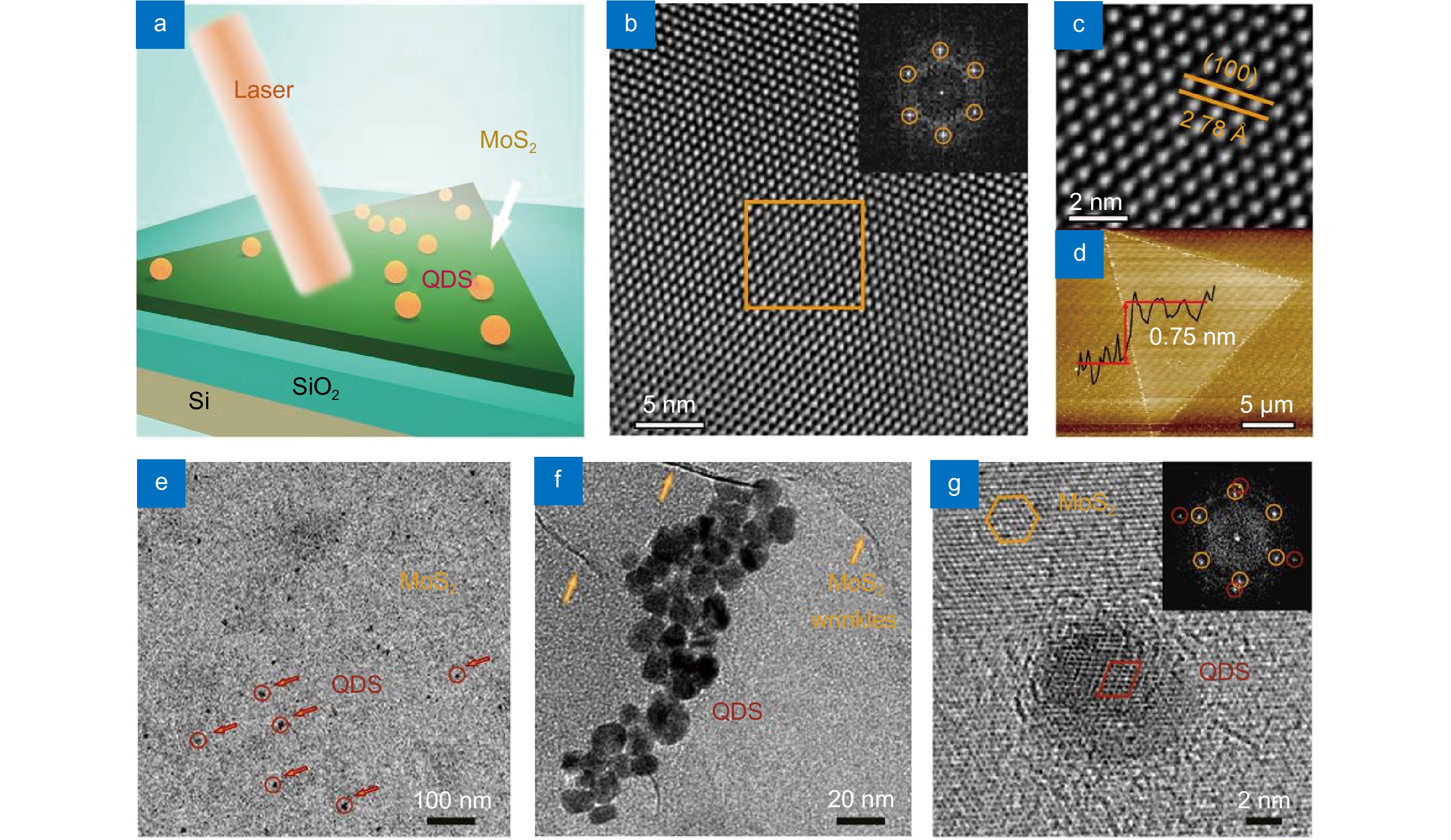
 DownLoad: